Low-power biasing networks for superconducting integrated circuits

a superconducting integrated circuit and biasing network technology, applied in the direction of superconductor devices, resistive material coatings, solid-state devices, etc., can solve problems such as system destabilization, maintain stability over a range of data sequences, and achieve high dynamic impedance

Active Publication Date: 2013-10-29
SEEQC INC
View PDF4 Cites 54 Cited by
  • Summary
  • Abstract
  • Description
  • Claims
  • Application Information

AI Technical Summary

Benefits of technology

[0076]A further object provides a superconducting integrated circuit, comprising a plurality of interconnected superconducting information processing elements, having an average bias voltage dependent on a data sequence, each being statically biased near to, but less than, a critical current for a superconducting junction of a respective superconducting information processing element and being associated with a dynamic power dissipation greater than two times a respective static power dissipation; and a biasing network comprising a superconducting inductor, configured to dynamically isolate and independently bias each of the superconducting information storage elements, while substantially isolating a dynamic bias state for each of the plurality of superconducting information storage elements, while maintaining stability over a range of data sequences.
[0077]A still further object provides a method of biasing a superconducting integrated circuit, comprising providing a plurality of superconducting junctions, having a data sequence dependent bias voltage and each being biased near to, but less than, a critical current for the respective junction; and biasing the plurality of superconducting junctions with a biasing network comprising a superconducting inductor, the biasing network having a static power dissipation of less than

Problems solved by technology

If the voltages on the current injection nodes were not equal, this would cause the cur

Method used


Image

  • Low-power biasing networks for superconducting integrated circuits
  • Low-power biasing networks for superconducting integrated circuits
  • Low-power biasing networks for superconducting integrated circuits

Examples


Embodiment Construction

[0093]The several preferred embodiments are hereby described in greater detail, with reference to the figures.

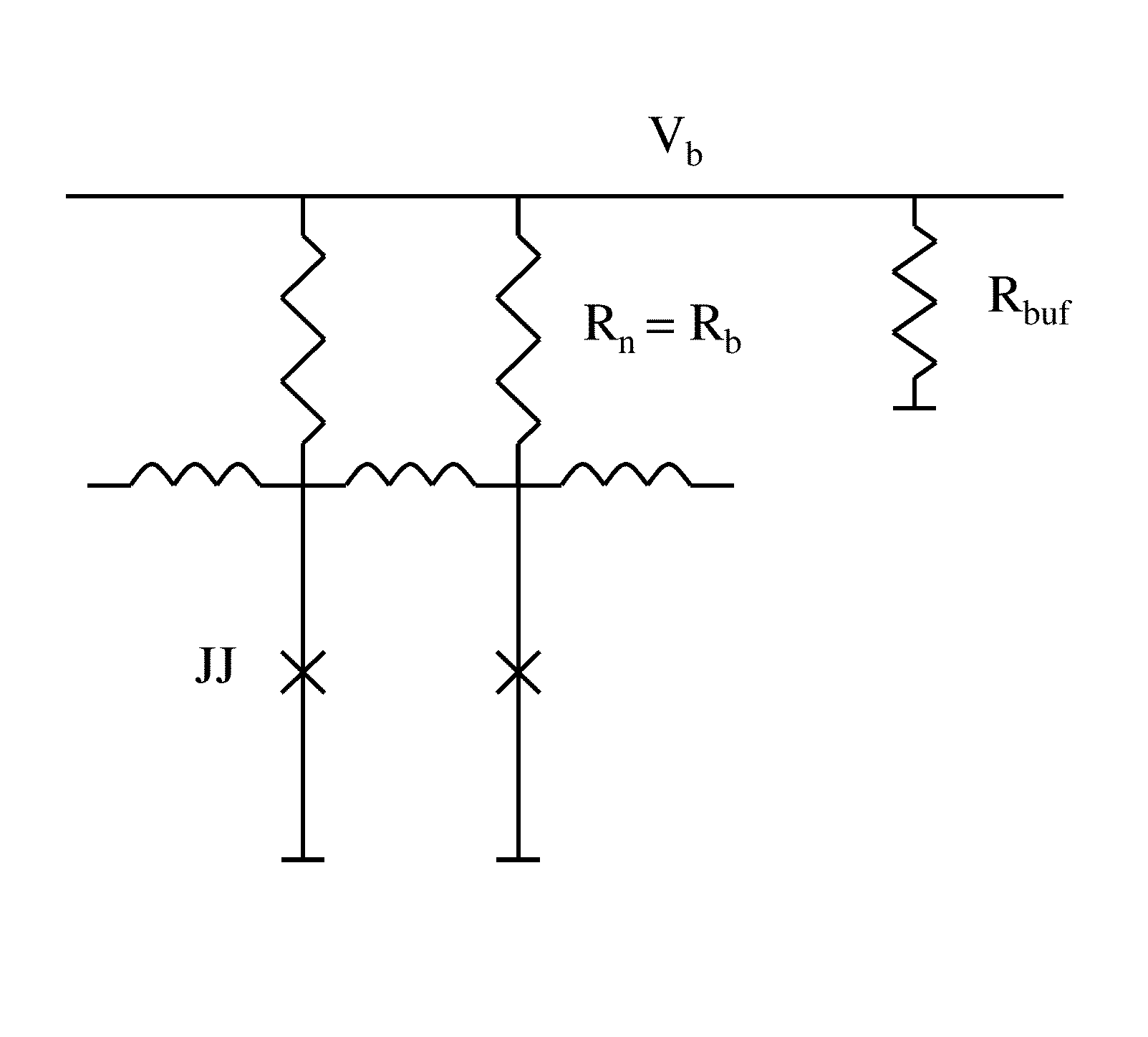
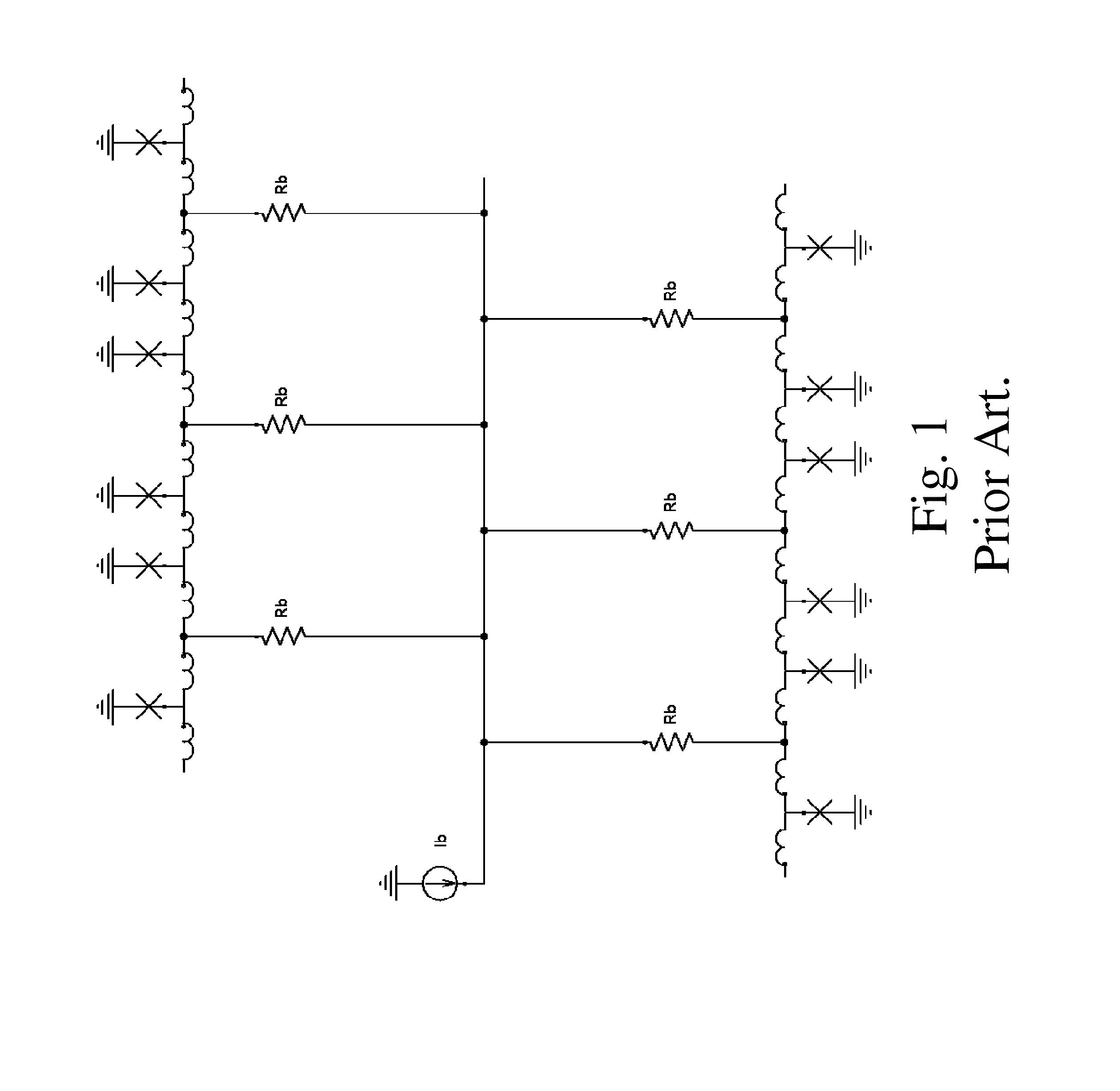
[0094]FIG. 1 of the prior art shows a current source providing bias current to two Josephson transmission lines (JTLs), one on the top and the other on the bottom. A JTL comprises a set of parallel Josephson junctions (each symbolized by ‘X’) connected by small inductors, and functions as an active transmission line for SFQ pulses.

[0095]A set of parallel resistors Rb is used to bias the set of JTLs at a constant current less than the critical current Ic of the junctions, so that there is no voltage or static power in the junctions. When an SFQ voltage pulse is introduced at one end of the JTL, it causes each junction in turn to exceed Ic in a transient fashion, generating an SFQ pulse which propagates to the next junction.

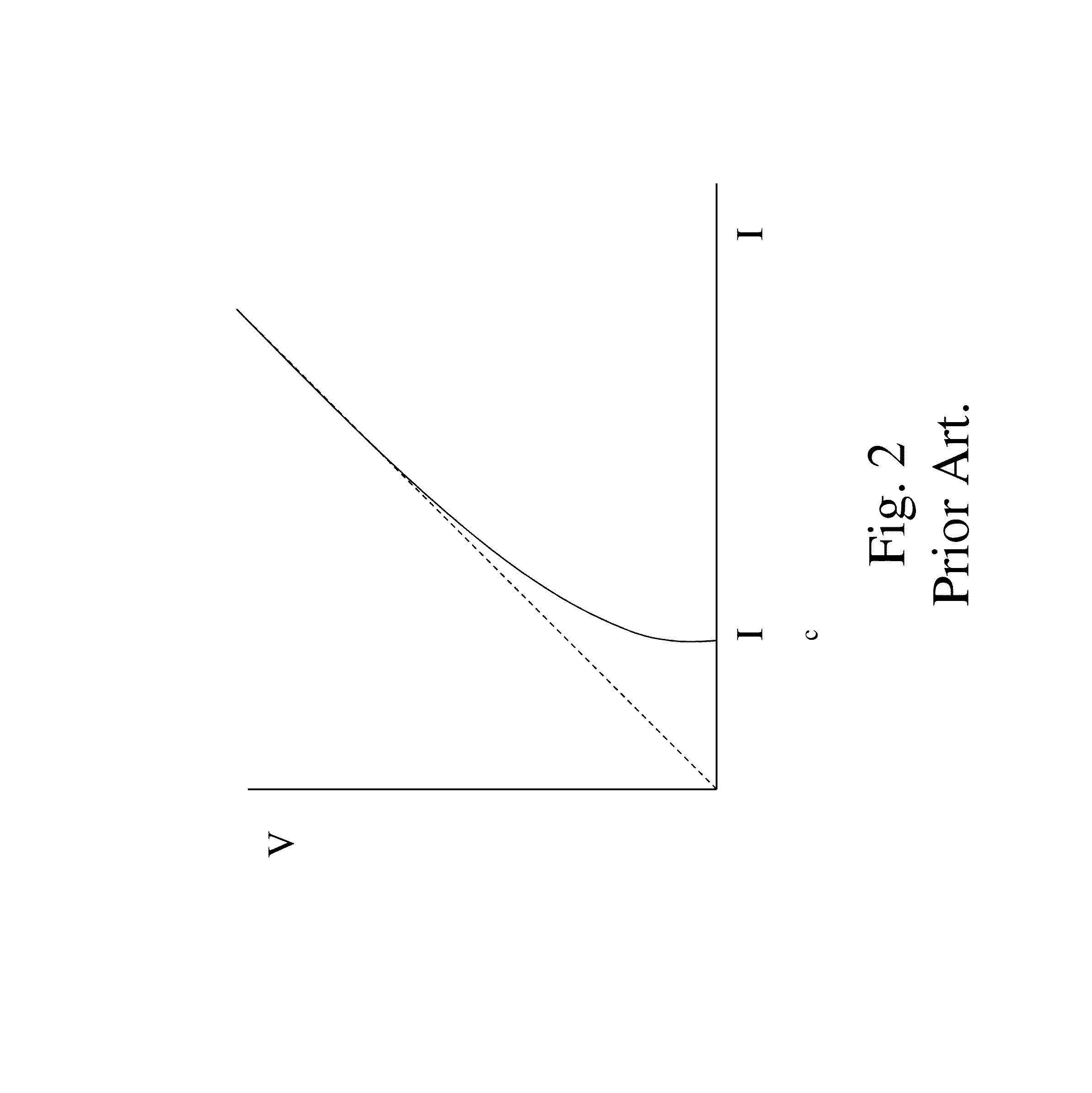
[0096]Each Josephson junction in FIG. 1 is actually a damped Josephson junction. While there are technologies whereby sufficient damping can be provided by...


PUM

PropertyMeasurementUnit
Electrical resistanceaaaaaaaaaa
Electrical inductanceaaaaaaaaaa
Currentaaaaaaaaaa

Abstract

A superconducting integrated circuit, comprising a plurality of superconducting circuit elements, each having a variation in operating voltage over time; a common power line; and a plurality of bias circuits, each connected to the common power line, and to a respective superconducting circuit element, wherein each respective bias circuit is superconducting during at least one time portion of the operation of a respective superconducting circuit element, and is configured to supply the variation in operating voltage over time to the respective superconducting circuit element.

Description

CROSS REFERENCE TO RELATED APPLICATIONS[0001]The present application claims benefit of priority from U.S. Provisional Patent Application No. 61 / 250,838, filed Oct. 12, 2009, the entirety of which is expressly incorporated herein by reference, and from U.S. Provisional Patent Application No. 61 / 369,927, filed Aug. 2, 2010, the entirety of which is expressly incorporated herein by referenceFIELD OF THE INVENTION[0002]The present invention relates to superconducting integrated circuits. In particular, it relates to biasing schemes for superconducting circuit elements.BACKGROUND OF THE INVENTION[0003]Active devices in integrated circuits require one or more power supplies. For many logic families, Direct Current (DC) power sources are required. Instead of supplying all possible values of voltage and current used in the circuit, a standard approach is to use networks of resistors to distribute the power among the various bias nodes of the circuit with appropriate values. This is the case...

Claims


Application Information

Patent Timeline
IPC IPC(8): H01L39/24H05K3/00H05K1/00
CPCH01L27/18H01L39/14H03K19/195Y10T29/49124H10N69/00H10N60/10H10N60/12H01B12/02H01B12/16H03K3/38
Inventor MUKHANOV, OLEG A.KIRICHENKO, ALEXANDER F.KIRICHENKO, DMITRI
Owner SEEQC INC
Why Eureka
Try Eureka