Pixel defect correction device, imaging apparatus, pixel defect correction method, and program

a defect correction and defect technology, applied in the field of pixel defect correction devices, imaging apparatuses, pixel defect correction methods, and programs, can solve the problems of difficult to perform edge detection precisely, degrading the precision of edge detection noticeably, and high possibility, so as to improve the accuracy of edge detection and improve the accuracy of defect detection

Active Publication Date: 2013-11-05
SONY SEMICON SOLUTIONS CORP
View PDF11 Cites 7 Cited by
  • Summary
  • Abstract
  • Description
  • Claims
  • Application Information

AI Technical Summary

Benefits of technology

[0013]In view of the above, it is desirable to provide a pixel defect correction device, an imaging apparatus, a pixel defect correction method, and a program capable of improving the edge detection precision and improving the defect detection precision.
[0018]According to the embodiments of the present invention, it is possible to improve the edge detection precision and as a result, to improve the defect detection precision.

Problems solved by technology

However, since the pixel value in the middle is not normal, there is a high possibility of degrading the precision of edge detection noticeably if the defective pixel itself is used for edge detection.
For example, in the methods disclosed in JP-A-2005-318383 and JP-A-2008-154276, even if not only a pixel whose defectiveness is to be determined but also the brightness value when a color carrier has been removed is used for edge detection, it is difficult to perform the edge detection precisely because a pixel of interest is not normal similar to that described above.

Method used


Image

  • Pixel defect correction device, imaging apparatus, pixel defect correction method, and program
  • Pixel defect correction device, imaging apparatus, pixel defect correction method, and program
  • Pixel defect correction device, imaging apparatus, pixel defect correction method, and program

Examples


first embodiment

[Example of the Entire Configuration of an Imaging Apparatus]

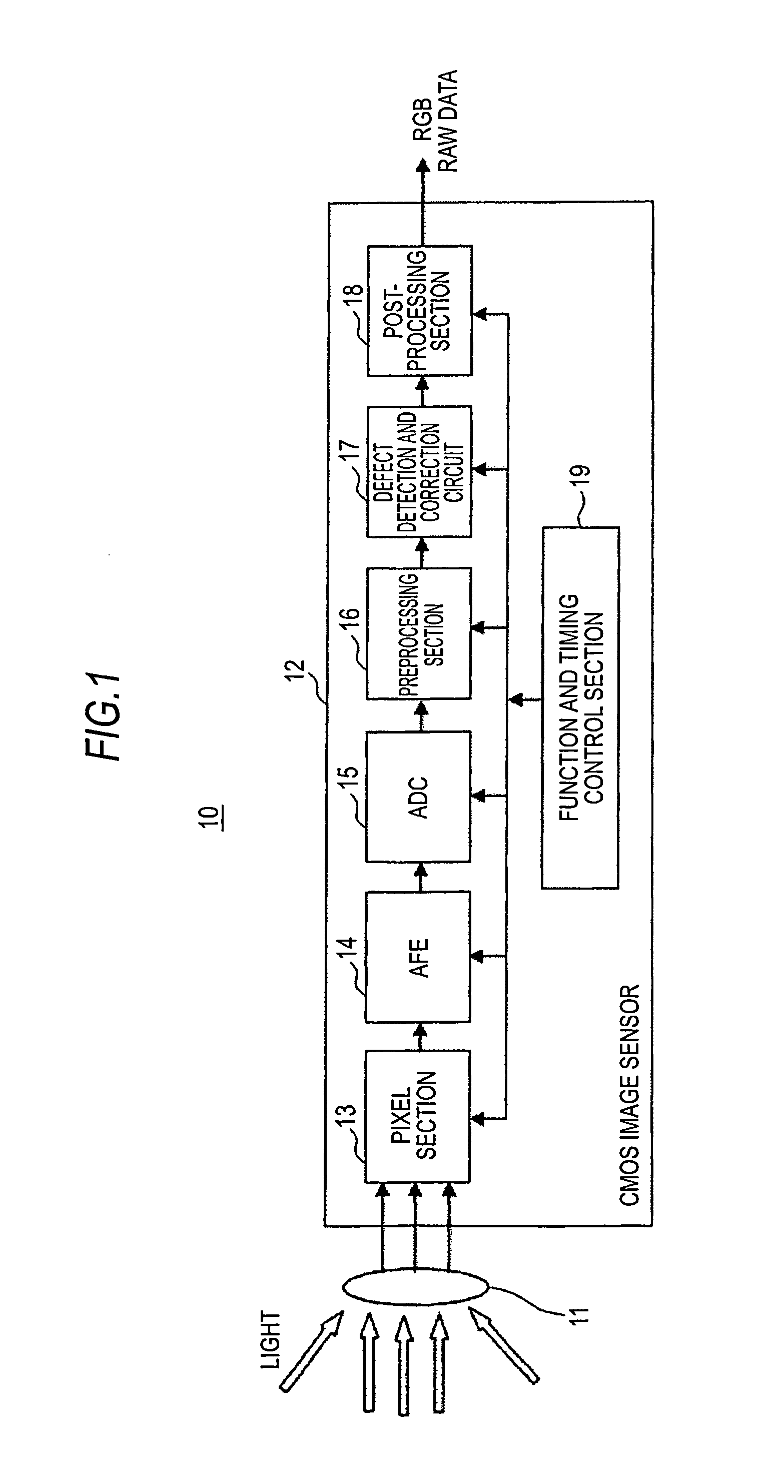
[0046]FIG. 1 is a block diagram showing an example of the configuration of an imaging apparatus to which a pixel defect correction device according to a first embodiment of the present invention is applied.

[0047]As shown in FIG. 1, an imaging apparatus 10 includes an optical system 11 and a CMOS image sensor 12 as a solid state imaging device.

[0048]The optical system 11 forms a subject image on the imaging surface of the imaging device 12.

[0049]The CMOS image sensor 12 includes a pixel section 13, an analog front end (AFE) 14, an analogue to digital converter (ADC) 15, and a preprocessing section 16.

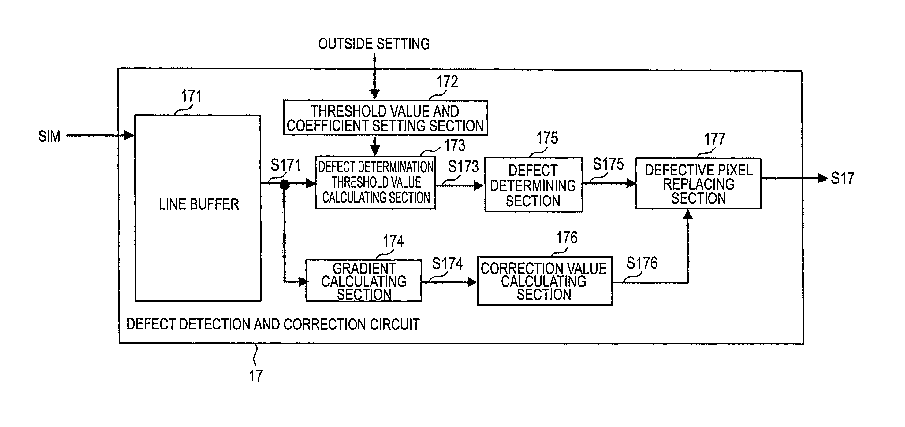
[0050]The CMOS image sensor 12 includes a defect detection and correction circuit 17 which adopts a pixel defect correction method according to the first embodiment of the present invention, a post-processing section 18, and a function and timing control section 19.

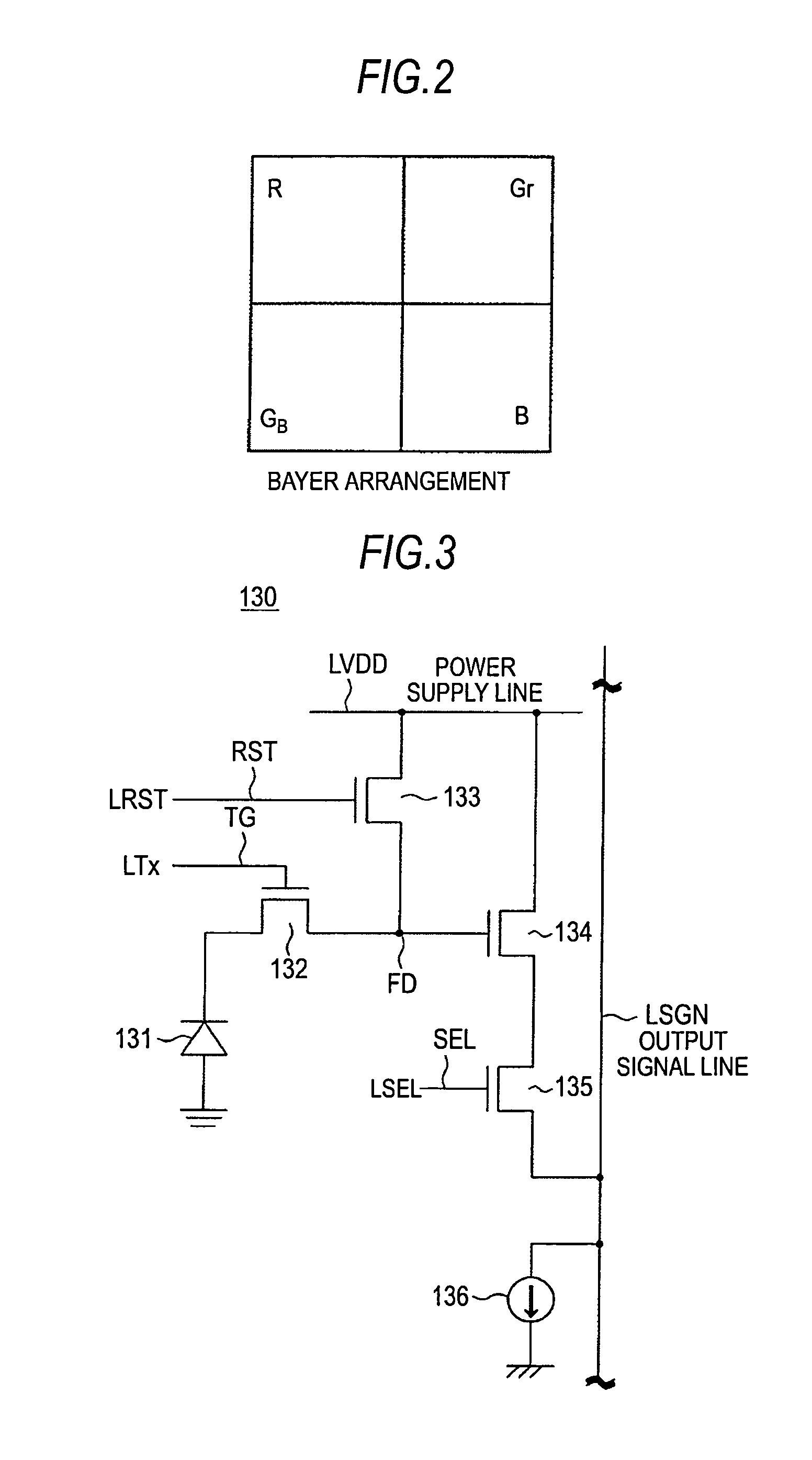
[0051]The pixel section 13 is formed by a CMOS sensor, and a pl...


PUM


Abstract

A pixel defect correction device includes: a defect determining section determining whether a pixel of interest of an image, in which pixels each having a pixel value are arrayed in a two-dimensional manner, is a defect of the image; a gradient detecting section detecting a gradient or an edge in a processing region, which includes pixels with the pixel of interest in the middle, based on values of at least peripheral pixels around the pixel of interest which are included in the processing region; a correction value acquisition section selecting a pixel, which is used for acquisition of a correction value of the pixel of interest, according to the detected gradient or edge and acquiring the correction value from a value of the selected pixel; and a defective pixel replacing section replacing the value of the pixel of interest with the correction value when the pixel of interest is determined to be a defect.

Description

BACKGROUND OF THE INVENTION[0001]1. Field of the Invention[0002]The present invention relates to a pixel defect correction device with a function of detecting and compensating for a defective pixel in a solid state imaging device, such as a CCD or a CMOS sensor, an imaging apparatus, a pixel defect correction method, and a program.[0003]2. Description of the Related Art[0004]Generally, it is known that a defective pixel is generated in a solid state imaging device, such as a CCD (Charge Coupled Device) and a CMOS (Complementary Metal Oxide Semiconductor) sensor.[0005]In such a solid state imaging device, it is known that a defective pixel, which outputs an abnormal imaging signal, is generated due to a local crystal defect of a semiconductor device and the like and this causes deterioration of the image quality.[0006]Examples of the defective pixel include a black defective pixel and a white defective pixel.[0007]That is, pixel defects of a solid state imaging device include a white...

Claims


Application Information

Patent Timeline
Patent Type & Authority Patents(United States)
IPC IPC(8): H04N5/367H04N9/45H04N5/361G06K9/00H04N9/64G06K9/40G06K9/48H04N5/208H04N5/228
CPCH04N5/3675H04N25/683
Inventor HASHIZUME, JUN
Owner SONY SEMICON SOLUTIONS CORP
Why Eureka
Try Eureka