NRAM arrays with nanotube blocks, nanotube traces, and nanotube planes and methods of making same

a technology of nanotubes and nanotube planes, applied in the field of carbon nanotube blocks, traces, layers and articles, can solve the problems of bipolar or fet switching elements in integrated circuits constructed from bipolar or fet switching elements, and the approach is limited to otp memories, and achieves the effect of low resistance and high resistance of nanotube articles

Active Publication Date: 2013-11-19
NANTERO
View PDF85 Cites 56 Cited by
  • Summary
  • Abstract
  • Description
  • Claims
  • Application Information

AI Technical Summary

Problems solved by technology

These requirements challenging the semiconductor industry to rapidly reduce geometries using improved process features.
While U.S. Pat. No. 4,442,507 introduces the concept of 3-D EPROM memory arrays having all cell components and interconnections decoupled from a semiconductor substrate, and above support circuits, the approach is limited to OTP memories.
Integrated circuits constructed from either bipolar or FET switching elements are typically volatile.
Alternative solutions to avoid losing information in volatile digital circuits, such as battery backup, also add cost and complexity to digital designs.

Method used


Image

  • NRAM arrays with nanotube blocks, nanotube traces, and nanotube planes and methods of making same
  • NRAM arrays with nanotube blocks, nanotube traces, and nanotube planes and methods of making same
  • NRAM arrays with nanotube blocks, nanotube traces, and nanotube planes and methods of making same

Examples


example fabrication

Techniques

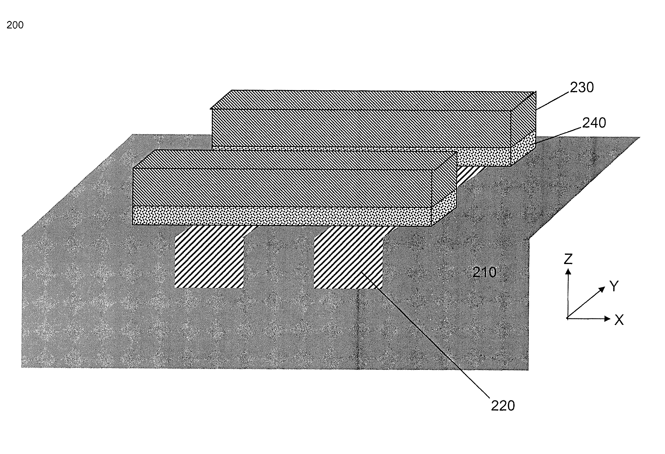
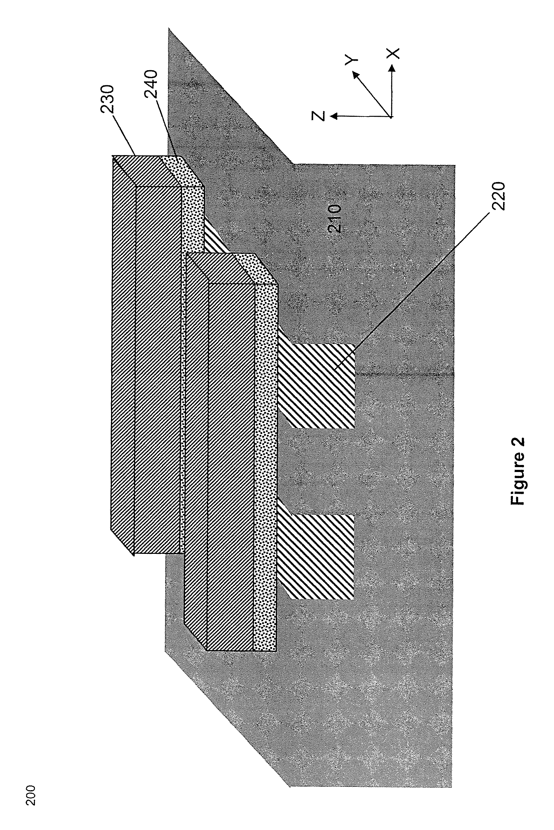
[0170]Fabrication techniques and processes for forming various NRAM systems, and nanotube blocks are described in great detail in the incorporated references. The following section provides certain variations on these techniques. These techniques are particularly useful for creating the aforementioned high-density structures, in which selected conductor layers (e.g. forming bit lines) are disposed over nanotube planes, traces, and blocks. The fabrication techniques described below may be implemented to form the 6F2 density memory cells as well as denser memory structures.

[0171]In certain embodiments, an additional material may be used to protect the CNT fabric during fabrication of a nanotube block. Protective materials may be disposed on a surface of a nanotube fabric, permeate a portion of the fabric itself, or provide some combination. In other words, the additional material may be used to protect an exterior surface of a nanotube fabric or may be used to form a CNT com...


PUM


Abstract

NRAM arrays with nanotube blocks, traces and planes, and methods of making the same are disclosed. In some embodiments, a nanotube memory array includes a nanotube fabric layer disposed in electrical communication with first and second conductor layers. A memory operation circuit including a circuit for generating and applying a select signal on first and second conductor layers to induce a change in the resistance of the nanotube fabric layer between the first and second conductor layers is provided. At least two adjacent memory cells are formed in at least two selected cross sections of the nanotube fabric and conductor layers such that each memory cell is uniquely addressable and programmable. For each cell, a change in resistance corresponds to a change in an informational state of the memory cell. Some embodiments include bit lines, word lines, and reference lines. In some embodiments, 6F2 memory cell density is achieved.

Description

CROSS REFERENCE TO RELATED APPLICATIONS[0001]This application claims priority under 35 U.S.C. §119(e) to U.S. Provisional Patent Appl. No. 61 / 074,241, filed on Jun. 20, 2008, entitled NRAM Arrays with Nanotube Blocks, Nanotube Traces, and Nanotube Planes and Methods of Making Same, which is herein incorporated by reference in its entirety.[0002]This application is related to the following applications, all of which are incorporated herein by reference in their entireties:[0003]U.S. Pat. No. 6,706,402, filed 23 Apr. 2002, entitled Nanotube Films and Articles;[0004]U.S. Pat. No. 6,835,591, filed 23 Apr. 2002, entitled Methods of Nanotube Films and Articles;[0005]U.S. patent application Ser. No. 11 / 280,786, filed 15 Nov. 2005, entitled Two-Terminal Nanotube Devices and Systems and Methods of Making Same;[0006]U.S. patent application Ser. No. 11 / 274,967, filed 15 Nov. 2005, entitled Memory Arrays Using Nanotube Articles with Reversible Nanoswitches;[0007]U.S. patent application Ser. No....

Claims


Application Information

Patent Timeline
Patent Type & Authority Patents(United States)
IPC IPC(8): G11C13/00
CPCB82Y10/00G11C13/025H01L27/2409H01L27/2436H01L27/2463H01L27/2472H01L45/04H01L45/1233H01L45/149H01L45/1675H10B63/20H10B63/82H10B63/30H10B63/80H10N70/20H10N70/826H10N70/8845H10N70/063
Inventor MANNING, H. MONTGOMERYRUECKES, THOMASBERTIN, CLAUDE L.WARD, JONATHAN W.DERDERIAN, GARO
Owner NANTERO
Why Eureka
Try Eureka