

Semiconductor device manufacturing method
a manufacturing method and semiconductor technology, applied in the manufacture of printed circuits, solid-state devices, basic electric elements, etc., can solve the problems of crack formation in the sealant resin body “f”, vaporization and expansion of moisture absorbed in the package “p”, and higher costs, so as to achieve the effect of increasing manufacturing costs
- Summary
- Abstract
- Description
- Claims
- Application Information
AI Technical Summary
Benefits of technology
Problems solved by technology
Method used
Image

Examples
Embodiment Construction
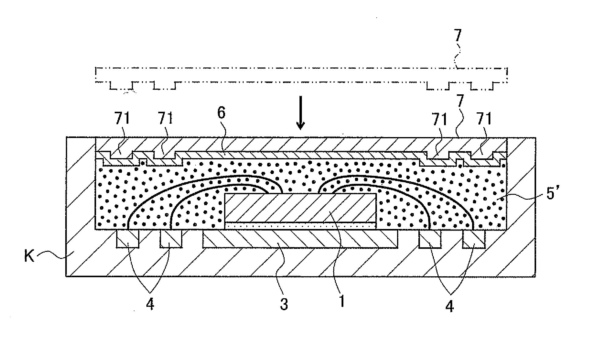
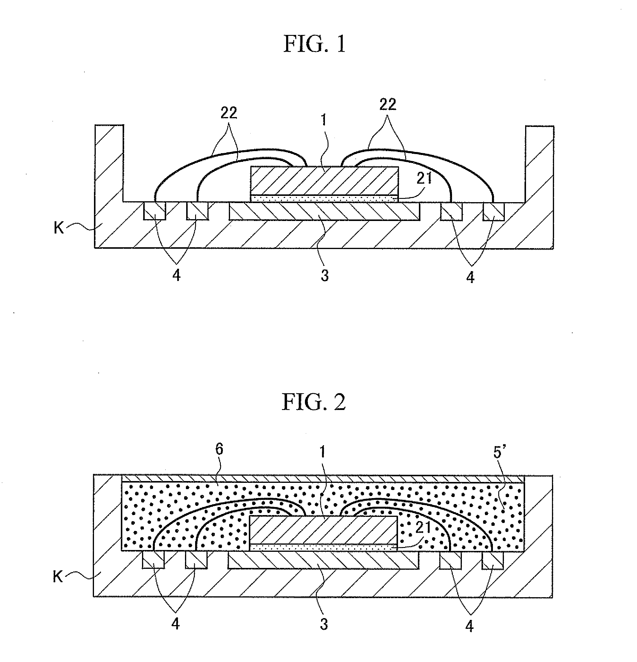
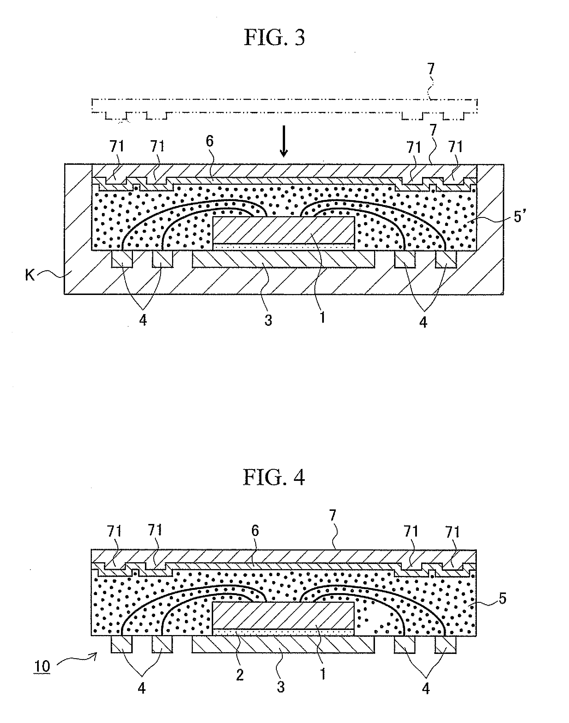
[0048]Embodiments of the present invention are described below with reference to the drawings. In addition, needless to say, the semiconductor device shown in each figure, the shapes of longitudinal sections of members constituting each device, the positions of semiconductor elements, electrodes, and the like are not limited to the examples in the drawings. Further, a semiconductor device may be accommodated in an exterior case.
[0049]FIGS. 1 to 3 schematically illustrate the flow of the first step of the semiconductor device manufacturing method of the present invention. FIG. 4 schematically illustrates a semiconductor package intermediate manufactured in the first step. In addition, FIG. 5 schematically illustrates the second step of the semiconductor device manufacturing method of the present invention. FIG. 6 schematically illustrates the third step of the semiconductor device manufacturing method of the present invention and one embodiment of a semiconductor device manufactured ...
PUM
 Abstract
Description
Claims
Application Information