Supercharge Your Innovation With Domain-Expert AI Agents!

Wiring board and method of manufacturing the same

a wiring board and manufacturing method technology, applied in the field of wiring boards, can solve the problems of lowering the possibility of a wiring portion being exposed, and achieve the effect of improving production yield and no additional cost burden

Active Publication Date: 2013-12-17
SHINKO ELECTRIC IND CO LTD
View PDF24 Cites 17 Cited by
  • Summary
  • Abstract
  • Description
  • Claims
  • Application Information

AI Technical Summary

Benefits of technology

The present invention provides a wiring board that is resistant to external mechanical stress and can prevent chipping or damage. This is achieved by reinforcing the peripheral region of the wiring board with a conductive layer, which increases its rigidity and makes it resistant to shock. This structure can also improve production yield without adding any additional manufacturing steps or cost.

Problems solved by technology

Moreover, the structure in which the board edge portion does not easily chip is implemented, so that the possibility of a wiring portion being exposed is lowered.

Method used


Image

  • Wiring board and method of manufacturing the same
  • Wiring board and method of manufacturing the same
  • Wiring board and method of manufacturing the same

Examples


Embodiment Construction

[0030]Hereinafter, descriptions are given of preferred embodiments of the present invention with reference to the accompanying drawings.

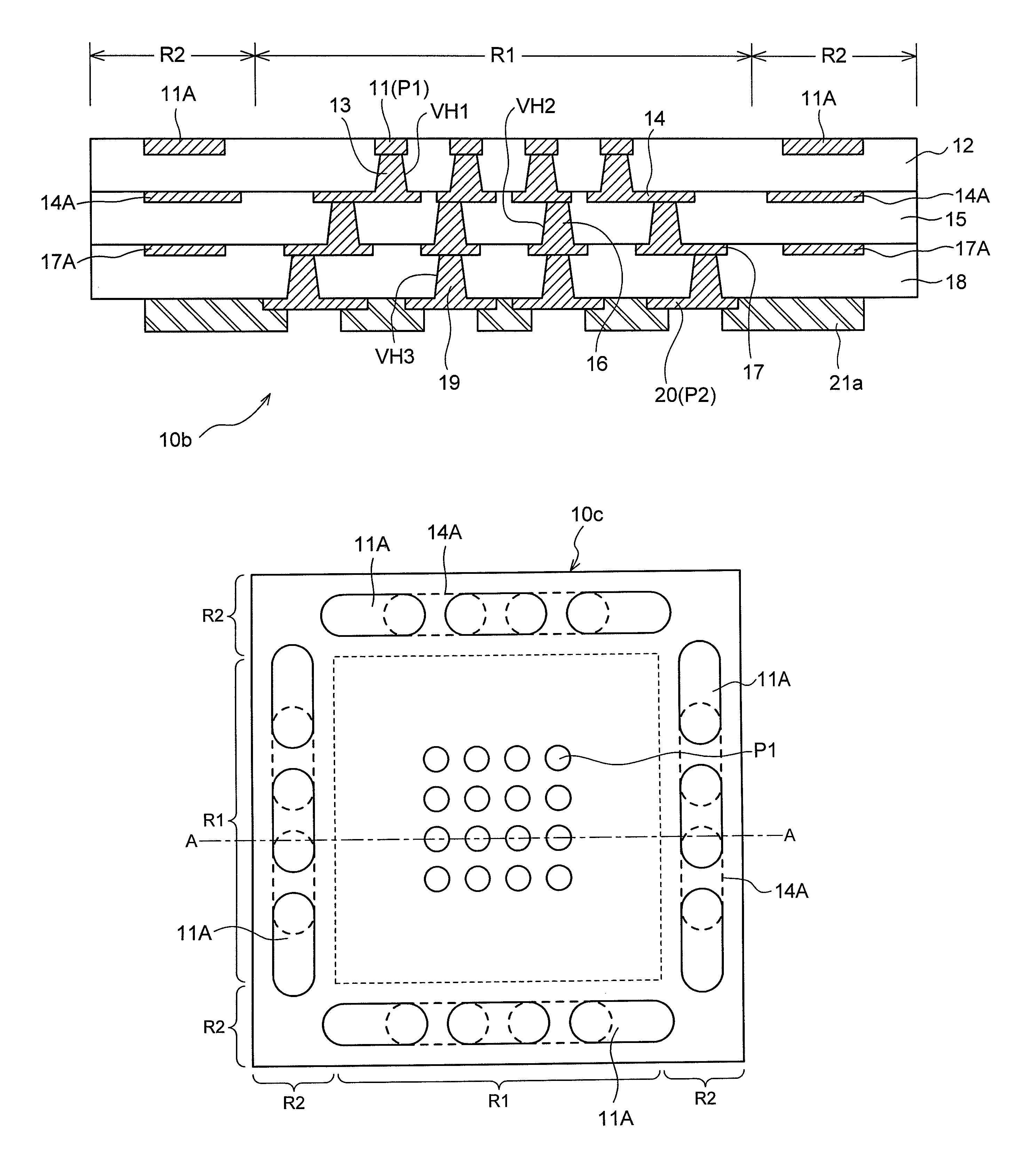
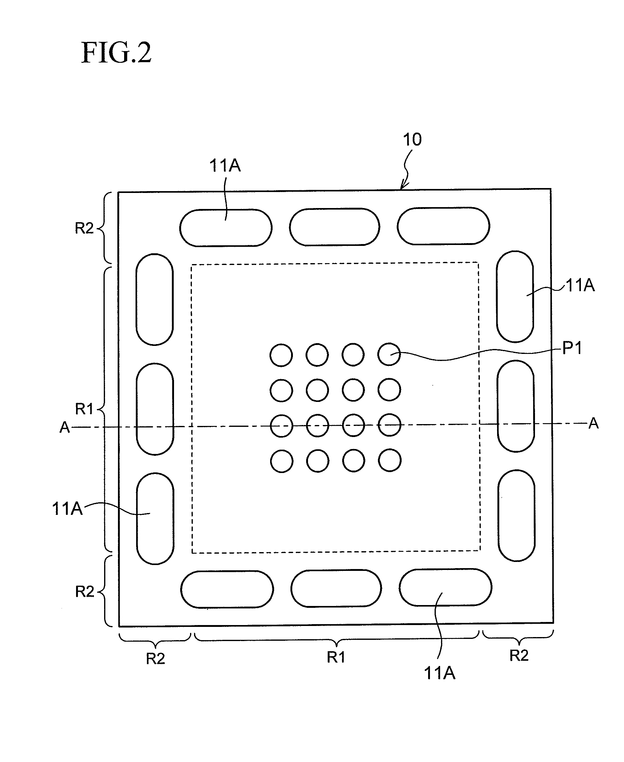
[0031]FIG. 1 shows a configuration of a wiring board (semiconductor package) 10 according to an embodiment of the present invention, in a cross-sectional view. FIG. 2 schematically shows in plan view, the configuration of the wiring board 10 when the wiring board 10 is viewed from an upper side (side on which an electronic component (chip) such as a semiconductor element is mounted) thereof. The cross-sectional view of FIG. 1 shows the configuration of the wiring board 10 as viewed in cross-sectional view along the line A-A in the plan view of FIG. 2.

[0032]The wiring board (semiconductor package) 10 according to the present embodiment has a structure in which multiple wiring layers 11, 14, 17 and 20 are stacked one on top of another with insulating layers (specifically, resin layers) 12, 15 and 18 each interposed between corresponding two of the wir...


PUM

PropertyMeasurementUnit
distanceaaaaaaaaaa
side lengthaaaaaaaaaa

Abstract

A wiring board (package) has a structure in which multiple wiring layers are stacked one on top of another with insulating layers each interposed between corresponding two of the wiring layers, and the wiring layers are connected to one another through vias formed in each of the insulating layers. In a peripheral region of the package, reinforcing patterns are provided on the same surfaces where the corresponding wiring layers are provided, respectively. Each of the reinforcing patterns is formed of a conductive layer formed on the same surface where the corresponding one of the wiring layers is provided, and is provided in an intermittent ring-like shape when viewed in a planar view.

Description

CROSS-REFERENCE TO RELATED APPLICATIONS[0001]This application is based on and claims priority of Japanese Patent Application No. 2009-006894 filed on Jan. 15, 2009, the entire contents of which are incorporated herein by reference.BACKGROUND OF THE INVENTION[0002](a) Field of the Invention[0003]The present invention relates to a wiring board for use in packaging an electronic component such as a semiconductor element and a method of manufacturing the same. More specifically, the invention relates to a wiring board having a structure in which multiple wiring layers are stacked one on top of another with an insulating layer interposed therebetween and are interconnected through vias formed in the insulating layers, and a method of manufacturing the same.[0004]The aforementioned wiring board is also referred to as a “semiconductor package” in the following description for the sake of convenience, because the wiring board serves as a package for mounting a semiconductor element or the l...

Claims


Application Information

Patent Timeline
Patent Type & Authority Patents(United States)
IPC IPC(8): H05K1/11H05K7/02
CPCH01L23/49838H05K1/113H05K3/4682H01L23/49822H01L23/49816Y10T29/49165H01L2221/68345H01L2224/16H01L2924/01078H01L2924/01079H01L2924/15174H01L2924/15311H05K3/205H01L2224/16225H01L2224/32225H01L2224/73204H01L2224/16235H01L2924/00H01L2224/16237H01L2924/00014H01L2924/00011H01L2224/0401
Inventor MIYASAKA, TOSHIJIHORIUCHI, AKIO
Owner SHINKO ELECTRIC IND CO LTD
Features
  • R&D
  • Intellectual Property
  • Life Sciences
  • Materials
  • Tech Scout
  • Unparalleled Data Quality
  • Higher Quality Content
  • 60% Fewer Hallucinations
Learn More