LED device and method for manufacturing the same

a technology of led devices and chromaticity, which is applied in the direction of semiconductor devices, basic electric elements, electrical equipment, etc., can solve the problems of color temperature and color temperature deviation of color temperature and dispersed chromaticity, and non-uniform illumination of led packages

Active Publication Date: 2014-02-11
ADVANCED OPTOELECTRONIC TECH INC
View PDF10 Cites 2 Cited by
  • Summary
  • Abstract
  • Description
  • Claims
  • Application Information

AI Technical Summary

Benefits of technology

[0024]The disclosure provides an LED device having multiple luminescent conversion layers, wherein the specific gravity of the first luminescent layer is greater than that of the second luminescent layer. Moreover, by virtue of the lateral light exciting the luminescent conversion elements which are at a lower specific gravity in the second luminescent layer, the intensity of any lateral light emitted from the luminescent conversion layer is enhanced to rival or be identical to the positive light emitted. Therefore, the LED device of the present disclosure has uniform illumination, stable color temperature and better-defined chromaticity. Furthermore, the manufacturing method for the LED device uses the screen with different meshes to sift luminescent conversion elements inside the luminescent layer to form multiple luminescent conversion layers with different specific gravities that leads to ease of mass production in manufacturing.

Problems solved by technology

In an LED package, an intensity of light emitted directly out in a plan view of an LED chip, the positive light, is greater than that of lateral-direction light which results in non-uniform illumination by the LED package.
Therefore, the LED package may cause the issues of non-uniform illumination deviation of color temperature and dispersed chromaticity.

Method used


Image

  • LED device and method for manufacturing the same
  • LED device and method for manufacturing the same
  • LED device and method for manufacturing the same

Examples


Embodiment Construction

[0009]Exemplary embodiments of the disclosure will be described with reference to the accompanying drawings.

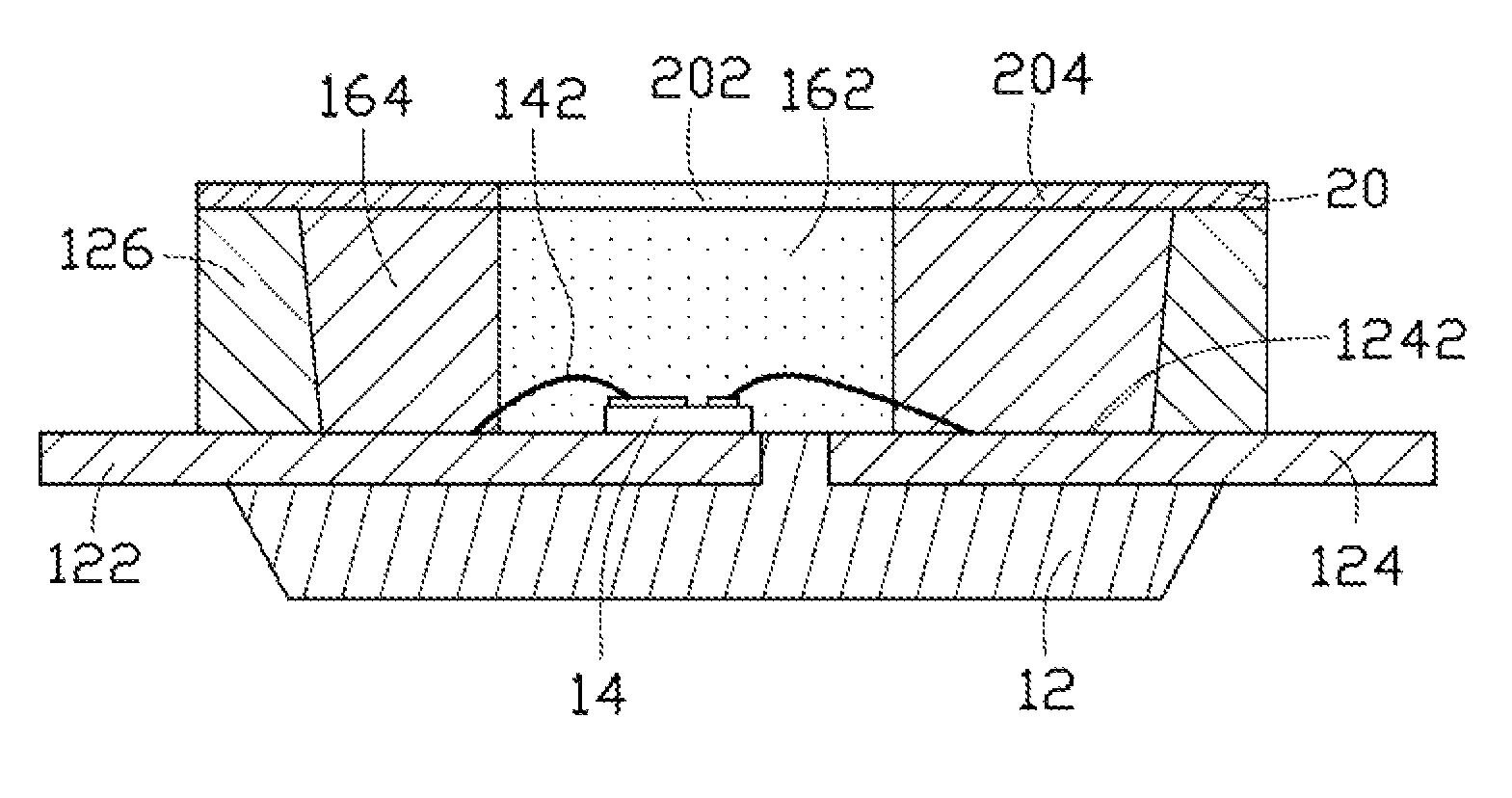
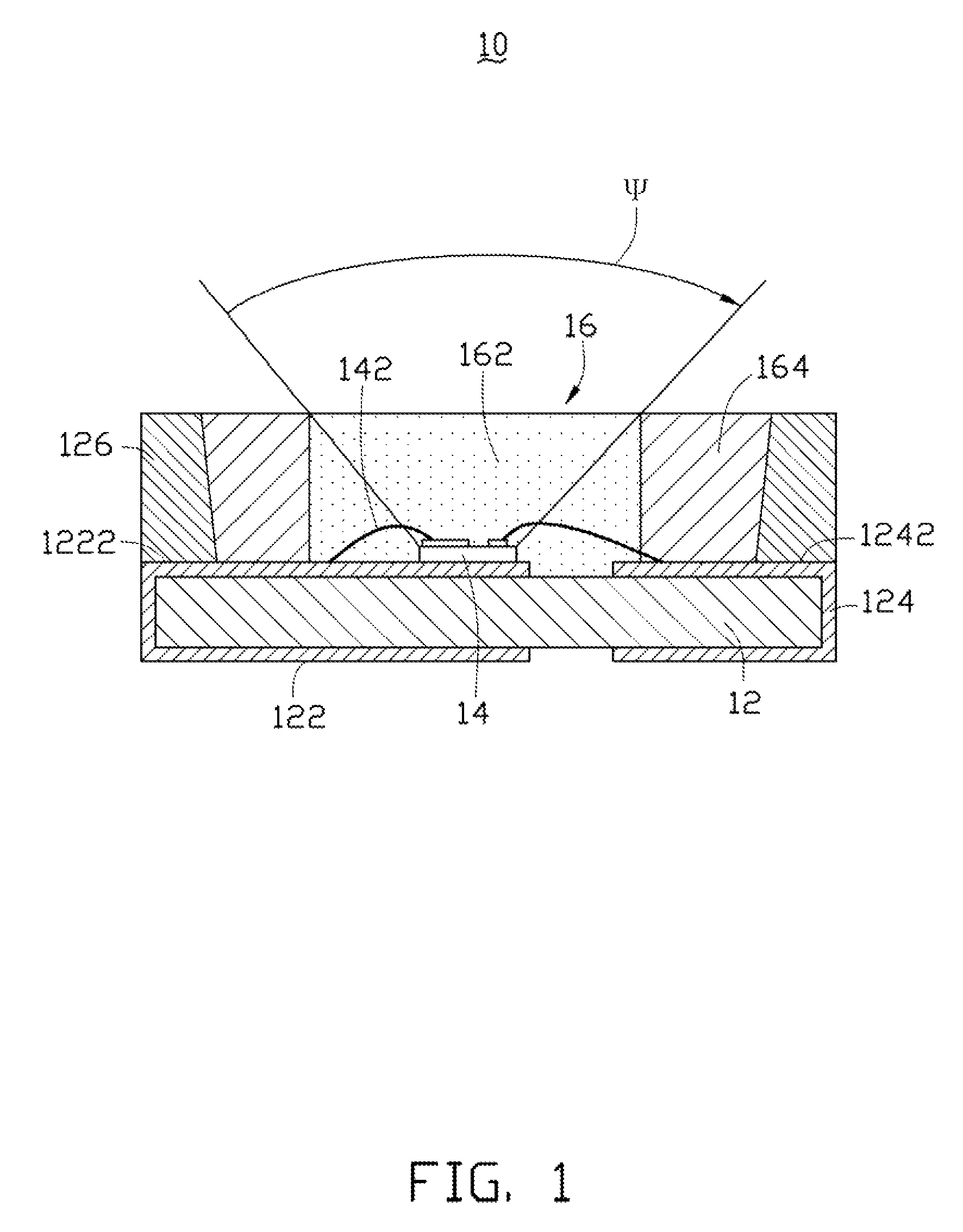
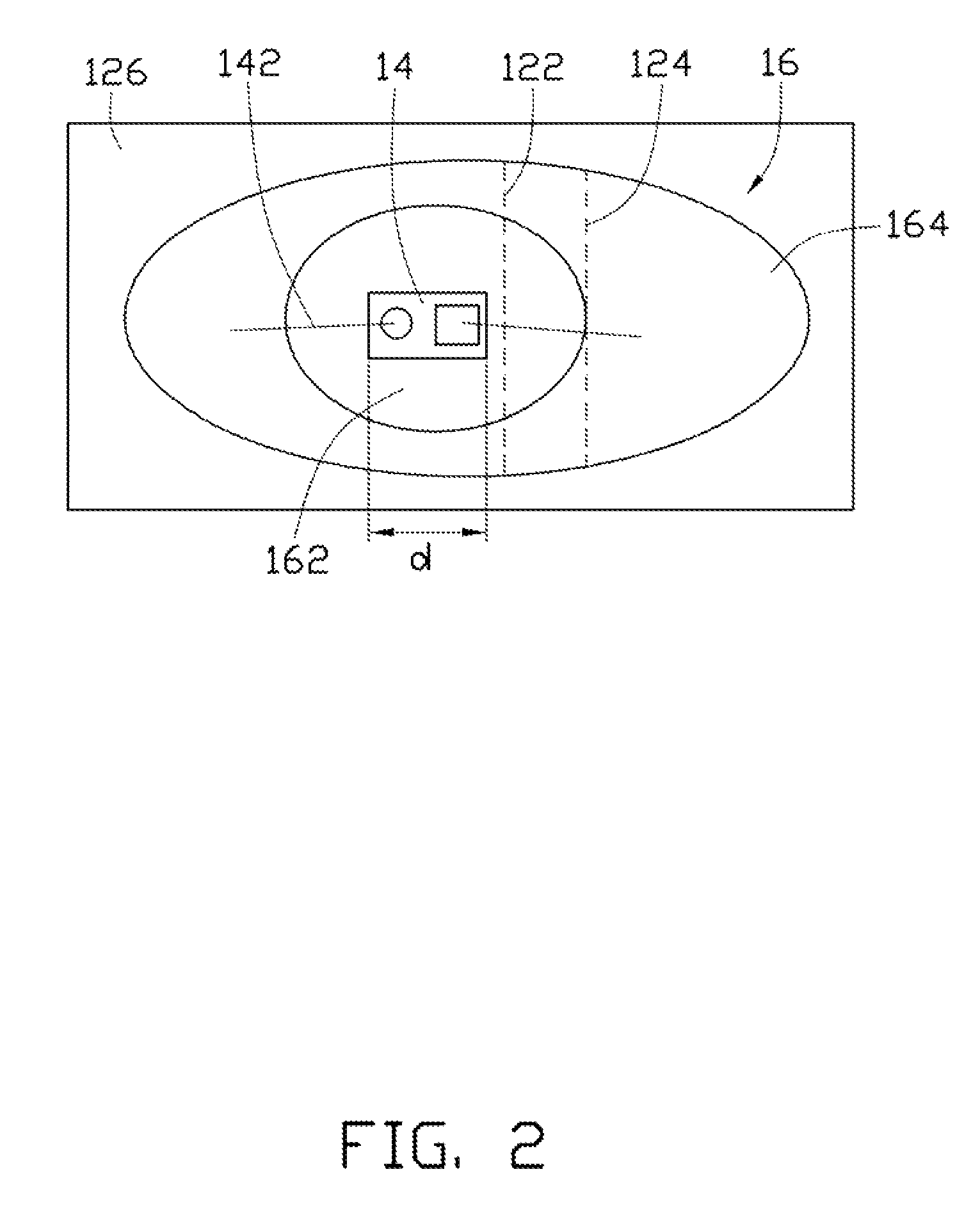
[0010]Referring to FIG. 1, the disclosure provides an LED device 10 comprising a substrate 12, an LED chip 14 and a luminescent conversion layer 16.

[0011]The substrate 12 comprises a first electrode 122, a second electrode 124 and a reflector 126. The first and the second electrode 122, 124 are opposite to each other, and respectively incorporate top faces 1222, 1242 above the substrate 12. The reflector 126 is located on the top faces 1222, 1242 and can be formed out of polymer, polyphthalamide (PPA) or plastic.

[0012]The LED chip 14 is disposed on the top face 1222 of the first electrode 122 surrounded by the reflector 126 and electrically connects to the first and the second electrodes 122, 124. In the disclosure, the LED chip 14 is connected to the first and the second electrode 122, 124 via conductive wires 142; alternatively, the LED chip 14 can be electrically connected ...


PUM


Abstract

An LED device comprises a substrate, an LED chip and a luminescent conversion layer. The substrate comprises a first electrode, a second electrode and a reflector located on top faces of the first and the second electrodes. The LED chip is disposed on the first electrode and electrically connected to the first and the second electrodes. The luminescent conversion layer is located inside the reflector and comprises a first luminescent conversion layer and a second luminescent conversion layer with different specific gravities. A manufacturing method for the LED device is also provided.

Description

TECHNICAL FIELD[0001]The disclosure relates generally to semiconductor devices, and more particularly to a light emitting device having high efficiency and uniform color temperature.DESCRIPTION OF THE RELATED ART[0002]Light emitting diodes (LEDs) have low power consumption, high efficiency, quick reaction time, long life and the absence of toxic elements such as mercury in their manufacture. In an LED package, an intensity of light emitted directly out in a plan view of an LED chip, the positive light, is greater than that of lateral-direction light which results in non-uniform illumination by the LED package. Moreover, a plurality of luminescent conversion elements evenly distributed around the LED chip may be excited by light emitted from the LED chip to produce light beams of shifted and different wavelengths. Therefore, the LED package may cause the issues of non-uniform illumination deviation of color temperature and dispersed chromaticity. A new LED device having high efficien...

Claims


Application Information

Patent Timeline
Patent Type & Authority Patents(United States)
IPC IPC(8): H01L21/00
CPCH01L33/504H01L2933/0025H01L33/60H01L33/505H01L2224/0603H01L2224/48091H01L2224/48247H01L2924/00014
Inventor CHANG, CHAO-HSIUNG
Owner ADVANCED OPTOELECTRONIC TECH INC
Why Eureka
Try Eureka