

Semiconductor memory device and method of manufacturing the same
a memory device and semiconductor technology, applied in the field of semiconductor devices, can solve the problems of leakage current and the limitation of the method of controlling the deterioration of leakage current characteristics, and achieve the effect of improving leakage current characteristics
- Summary
- Abstract
- Description
- Claims
- Application Information
AI Technical Summary
Benefits of technology
Problems solved by technology
Method used
Image

Examples
first embodiment
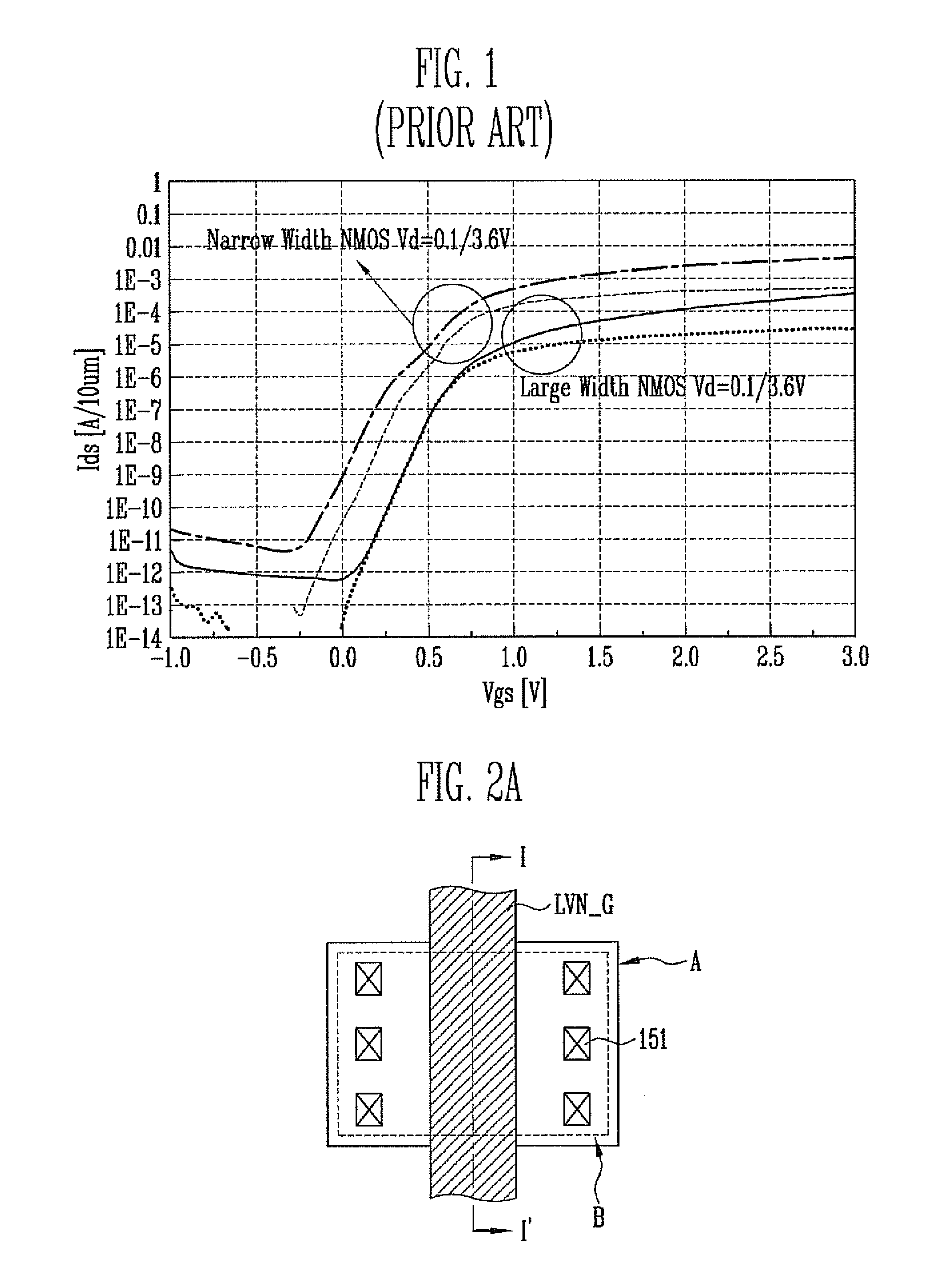
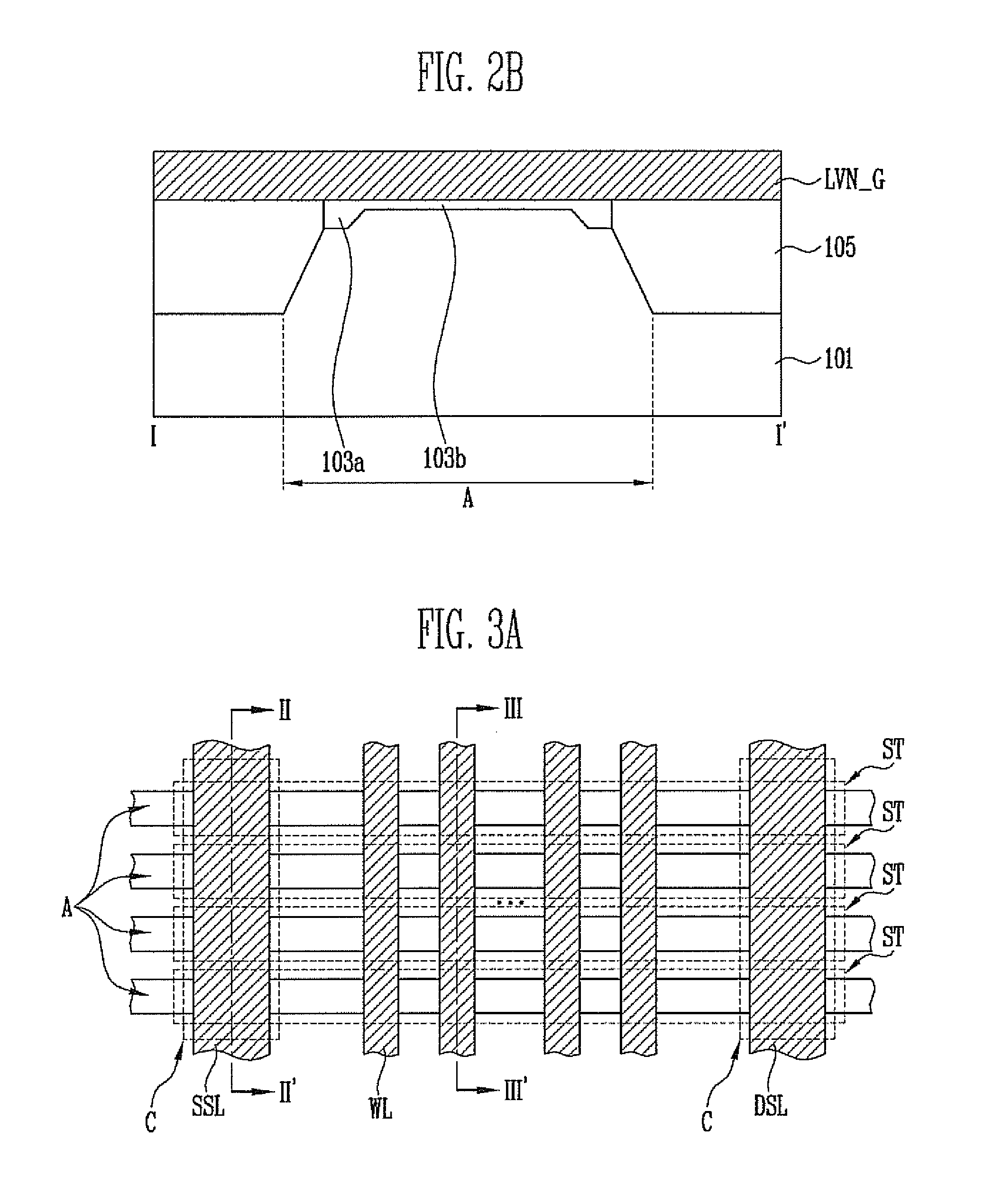
[0023]FIG. 2A is a plan view of a transistor of a semiconductor device according to the present invention. FIG. 2B is a cross-sectional view of the transistor of the semiconductor device taken along line “I-I′” of FIG. 2A. FIGS. 2A and 2B illustrate a low voltage NMOS transistor that is formed in a peripheral region of a flash memory device.
[0024]Referring to FIGS. 2A and 2B, the transistor of the semiconductor device according to the first embodiment of the present invention includes an active region A separated by an isolation layer 105, and the transistor is formed on top of a semiconductor substrate 101 into which well forming impurities and threshold voltage controlling impurities are implanted. In addition, the transistor according to the first embodiment of the present invention includes a first gate insulating layer 103a having a first thickness, a second gate insulating layer 103b having a second thickness smaller than the first thickness, a gate LVN_G formed on top of the ...
second embodiment
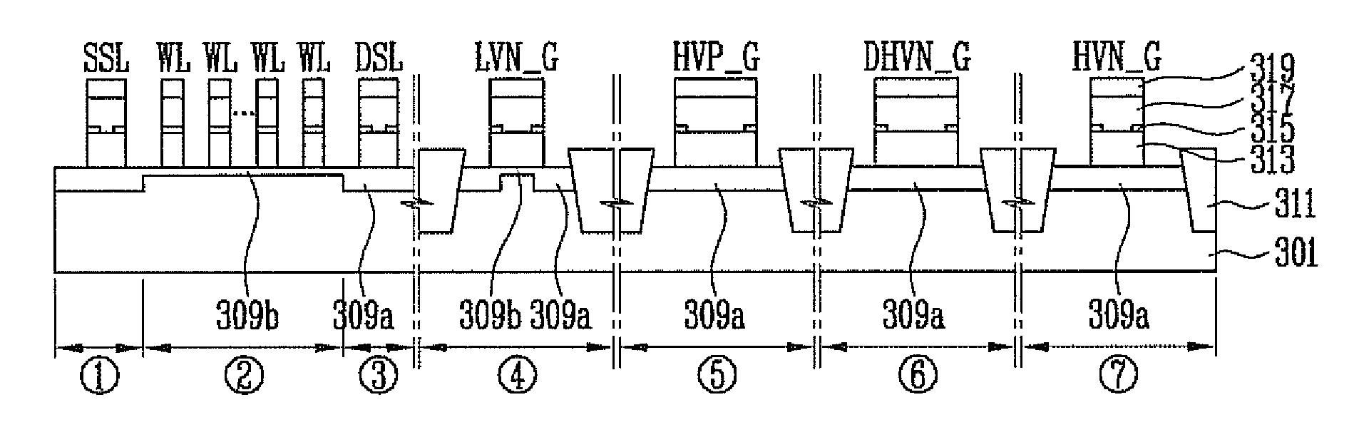
[0027]FIG. 3A is a plan view of transistors of a semiconductor device according to the present invention. FIG. 3B is a cross-sectional view of the transistors of the semiconductor device taken along line “II-II′” of FIG. 3A. FIG. 3C is a cross-sectional view of the transistors of the semiconductor device taken along line “III-III′” of FIG. 3A. FIGS. 3A to 3C together illustrate a portion of a cell array region of a flash memory device. Though FIG. 3B illustrates a cross-section taken in a direction of a source select line, a cross-section taken in a direction of a drain select line is the same as that of FIG. 3B.
[0028]As shown in FIG. 3A, memory strings ST are formed in a cell array region of a flash memory device. Each of the memory strings ST has a source select transistor, a plurality of memory cell transistors, and a drain select transistor that are arranged in a line on an active region A. The memory cell transistors are coupled in series between the source select transistor an...
third embodiment
[0048]FIG. 5A is a plan view of a transistor of a semiconductor device according to the present invention. FIG. 5B is a cross-sectional view of the transistor of the semiconductor device taken along line “IV-IV′” of FIG. 5A. FIGS. 5A and 5B particularly illustrate a low voltage NMOS transistor that is formed in a peripheral region of a flash memory device.
[0049]Referring to FIGS. 5A and 5B, according to the third embodiment of the present invention, the transistor of the semiconductor device includes an active region A that is separated by an isolation layer 405, and the transistor is formed on top of a semiconductor substrate 401 into which well forming impurities and threshold voltage controlling impurities are implanted.
[0050]The type and concentration of the threshold voltage controlling impurities and impurity implantation energy thereof vary according to transistor types. For example, when the semiconductor substrate 401 includes a high voltage NMOS transistor region, a low vo...
PUM
 Abstract
Description
Claims
Application Information