

Method for fabricating capacitor in semiconductor device
- Summary
- Abstract
- Description
- Claims
- Application Information
AI Technical Summary
Benefits of technology
Problems solved by technology
Method used
Image

Examples
Embodiment Construction
[0015]Hereinafter, a preferred embodiment of the present invention will be described with reference to the accompanying drawings. In the following description and drawings, the same reference numerals are used to designate the same or similar components, and so repetition of the description on the same or similar components will be omitted.
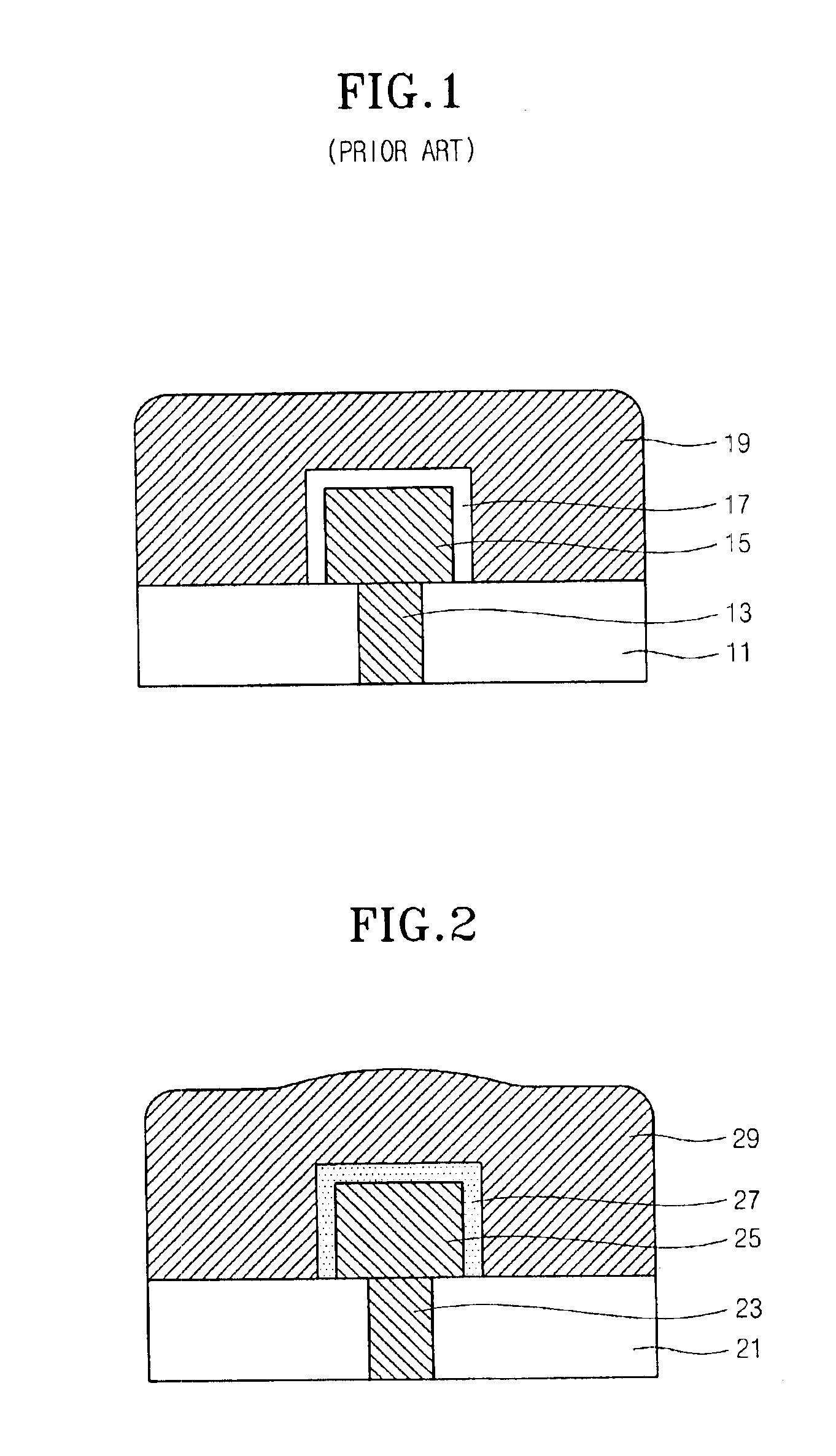
[0016]As shown in FIG. 2, with regards a method for fabricating a capacitor in a semiconductor device in accordance with the present invention, an interlayer insulating layer 21 is deposited on a wafer (not shown) wherein several elements are constructed, and selective patterning of the interlayer insulating layer is performed to thereby form a contact hole (not shown) exposing a part of the semiconductor wafer.
[0017]Then, a contact plug 23 is formed in the contact hole (not shown), and a storage node 25 of a cylindrical shape, a concave shape, etc., is formed on the entire surface of the semiconductor wafer.
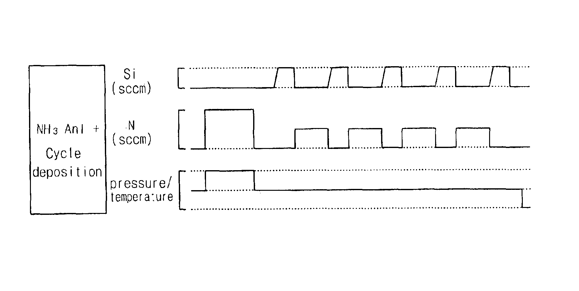
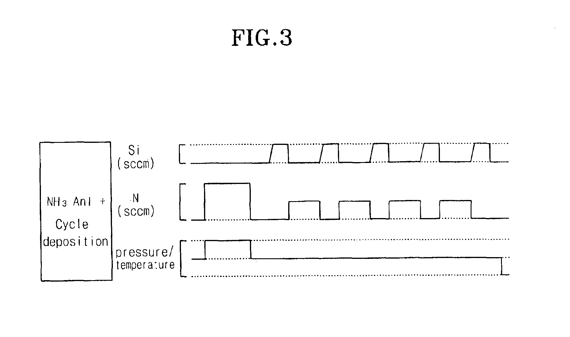
[0018]Next, a dielectric layer 27 made ...
PUM
| Property | Measurement | Unit |
|---|---|---|
| Temperature | aaaaa | aaaaa |
| Temperature | aaaaa | aaaaa |
| Temperature | aaaaa | aaaaa |
Abstract
Description
Claims
Application Information