Metal-Insulator-Metal (MIM) Capacitors Formed Beneath First Level Metallization and Methods of Forming Same

a technology of metal-insulator metal and capacitors, which is applied in the field of metal-insulator-metal (mim) capacitors and methods of forming same, can solve the problems of metal electrodes, lower mim capacitance, and variation in capacitors, and achieve the effect of improving the leakage current characteristics of capacitor dielectrics

Inactive Publication Date: 2007-02-15
SAMSUNG ELECTRONICS CO LTD
View PDF7 Cites 18 Cited by
  • Summary
  • Abstract
  • Description
  • Claims
  • Application Information

AI Technical Summary

Benefits of technology

[0008] Still further embodiments of the present invention include methods of forming an integrated circuit device by forming a metal-insulator-metal (MIM) capacitor on an integrated circuit substrate and forming an inter-metal dielectric (IMD) layer on the MIM capacitor. The IMD layer is then patterned to define a first opening therein that exposes an upper surface of a first electrode of the MIM capacitor. A first copper interconnect pattern is formed in the first opening using a copper damascene process. In some of these embodiments, the first copper interconnect pattern may be part of a dual-damascene interconnect structure associated with a lowermost level of copper metallization (e.g., M1 wiring layer). In further embodiments, the step of forming an inter-metal dielectric layer is preceded by a step of heat treating a dielectric layer of the MIM capacitor at a temperature in a range from about 300° C. to about 500° C. This heat treatment, which may be performed in an oxidizing ambient (e.g., an oxygen containing plasma), is performed for a sufficient duration to improve the leakage current characteristics of the capacitor dielectric within the MIM capacitor. The heat treatment may also be performed for a sufficient duration to increase a dielectric constant of the capacitor dielectric within the MIM capacitor.

Problems solved by technology

Moreover, the biasing of silicon electrodes, including single crystal silicon and poly-Si electrodes, can cause the formation of depletion regions therein that cause capacitance variations, which are a function of applied voltage.
Unfortunately, efforts to improve MIM capacitor performance using heat treatment may cause metal electrode oxidation, which can lower MIM capacitance.

Method used


Image

  • Metal-Insulator-Metal (MIM) Capacitors Formed Beneath First Level Metallization and Methods of Forming Same
  • Metal-Insulator-Metal (MIM) Capacitors Formed Beneath First Level Metallization and Methods of Forming Same
  • Metal-Insulator-Metal (MIM) Capacitors Formed Beneath First Level Metallization and Methods of Forming Same

Examples


first embodiment

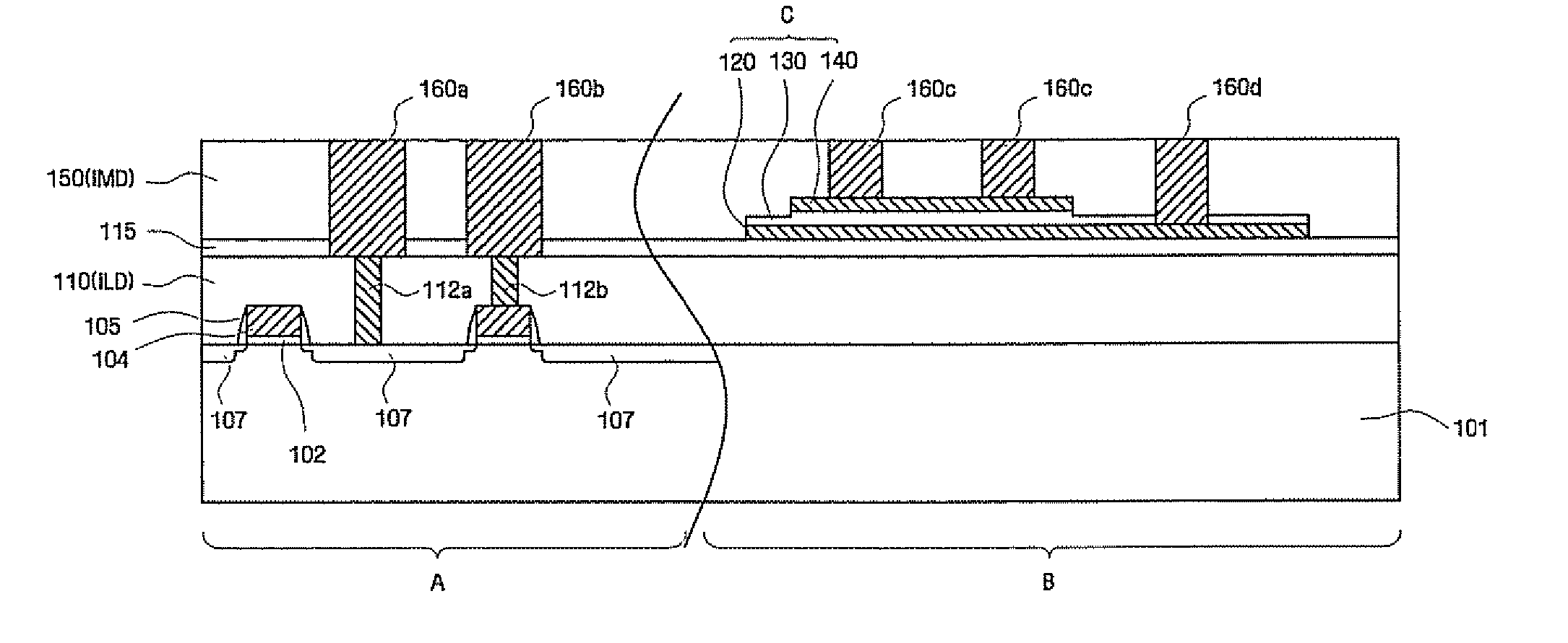
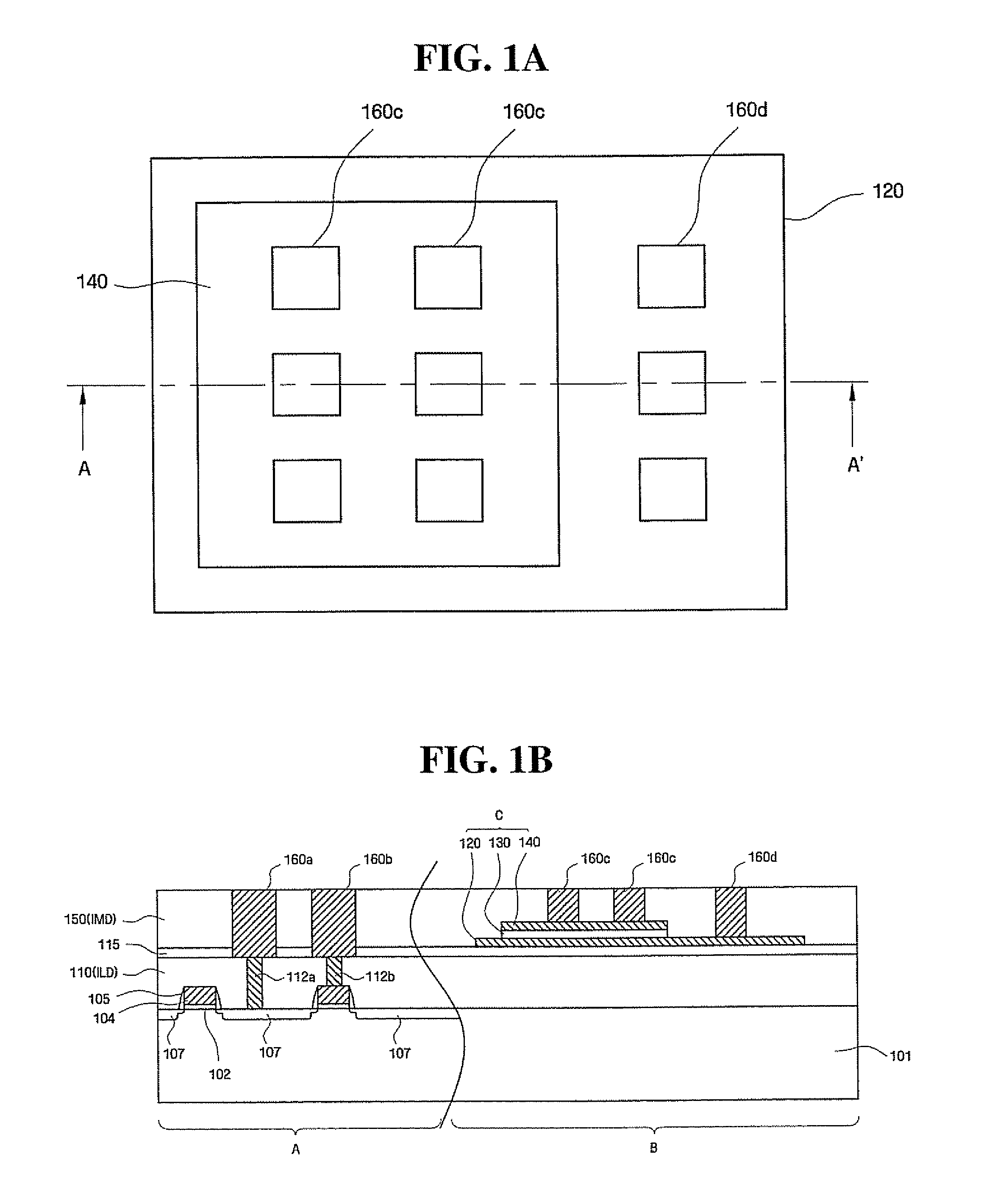
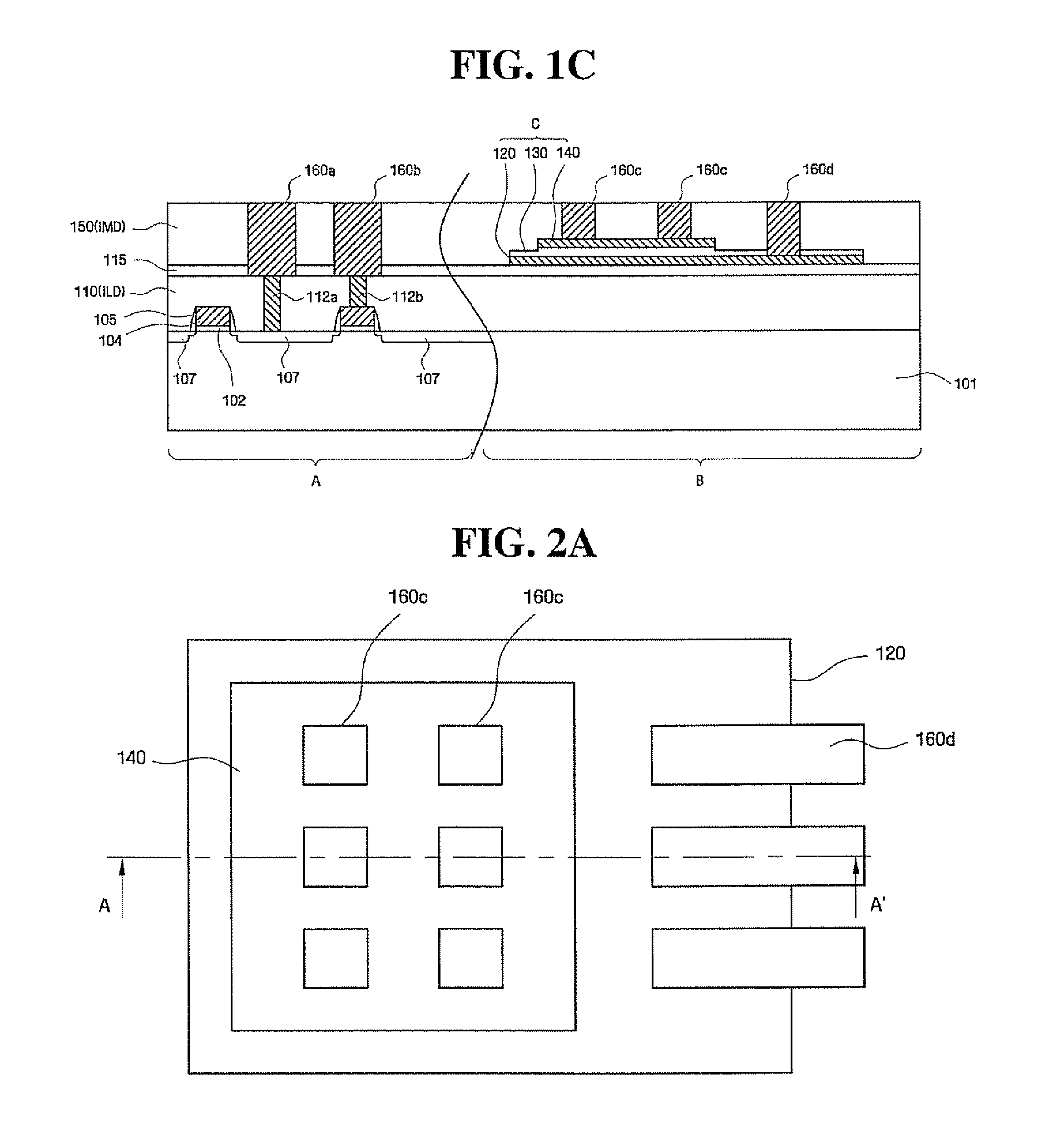
[0021] Referring now to FIG. 1A, an integrated circuit capacitor according to the invention is illustrated as including a lower capacitor electrode 120, an upper capacitor electrode 140 and a plurality of copper damascene interconnect patterns 160c and 106d, which are electrically connected to the upper and lower capacitor electrodes 140 and 120, respectively. As illustrated by FIGS. 1B and 1C, an integrated circuit chip may include a first semiconductor region A and a second semiconductor region B therein. The first semiconductor region A may be a memory cell array region of an integrated circuit memory device and the second region B may be a peripheral circuit region. The first semiconductor region A is shown as including active devices therein. These active devices (e.g., MOS transistors) include insulated gate electrodes (regions 102, 104) with sidewall insulating spacers 105, and source / drain regions 107 of first conductivity type (e.g., N-type) within a semiconductor substrate...

second embodiment

[0024] Referring now to FIGS. 2A-2B, an integrated circuit capacitor according to the invention is illustrated as including a lower capacitor electrode 120, an upper capacitor electrode 140 and a plurality of copper damascene interconnect patterns 160c and 106d, which are electrically connected to the upper and lower capacitor electrodes 140 and 120, respectively. The interconnect patterns 160d illustrated in FIGS. 2A-2B are of larger dimension relative to the interconnect patterns 160d illustrated by FIGS. 1A-1C. As illustrated by FIG. 2B, an integrated circuit chip may include a first semiconductor region A and a second semiconductor region B therein. The first semiconductor region A may be a memory cell array region of an integrated circuit memory device and the second region B may be a peripheral circuit region. The first semiconductor region A is shown as including active devices therein. These active devices (e.g., MOS transistors) include insulated gate electrodes (regions 10...

third embodiment

[0025] Referring now to FIGS. 3A-3B, an integrated circuit capacitor according to the invention is illustrated as including a lower capacitor electrode 120 and an upper capacitor electrode 140 of equivalent dimension. In addition, a semiconductor region 108 of first conductivity type is provided in the substrate 101 and a plurality of electrically conductive vias 112c (e.g., tungsten vias) are provided to electrically connect the semiconductor region 108 to the lower capacitor electrode 120. These vias 112a are provided within openings in the interlayer dielectric layer 110, as illustrated. Based on this configuration, the application of a potential bias (e.g., voltage) to the semiconductor region 108 will be transferred to the lower capacitor electrode 120.

[0026] Referring now to FIGS. 4A-4E, methods of forming the integrated circuit capacitors of FIGS. 1A-1C include forming a plurality of MOS transistors in a memory cell region A of an integrated circuit substrate 101. These MOS t...


PUM


Abstract

A metal-insulator-metal (MIM) capacitor for an integrated circuit may be provided on the interlayer insulating layer and covered by a inter-metal dielectric (IMD) layer. This IMD layer has at least a first opening therein that exposes an upper surface of a first electrode of the MIM capacitor. This first opening is filled with a first copper damascene interconnect pattern, which may in some embodiments be part of a dual-damascene copper interconnect structure associated with a first and lowermost level of metallization (e.g., M1 wiring layer). This first copper damascene interconnect pattern may have an upper surface that is planar with an upper surface of the IMD layer and a bottom surface that is in contact with the upper surface of the first electrode of the MIM capacitor.

Description

REFERENCE TO PRIORITY APPLICATION [0001] This application claims priority to Korean Patent Application No. 2005-74006, filed Aug. 11, 2005, the disclosure of which is hereby incorporated herein by reference. FIELD OF THE INVENTION [0002] The present invention relates to integrated circuit capacitors and, more particularly, to metal-insulator-metal (MIM) capacitors and methods of forming MIM capacitors. BACKGROUND OF THE INVENTION [0003] Integrated circuit capacitors include metal-oxide-semiconductor (MOS) capacitors, P-N junction capacitors, polySi-insulator-polySi (PIP) capacitors and metal-insulator-metal (MIM) capacitors. Of these types of capacitors, MIM capacitors offer enhanced characteristics because single crystal silicon electrodes and polysilicon electrodes typically have higher resistance compared to metal electrodes. Moreover, the biasing of silicon electrodes, including single crystal silicon and poly-Si electrodes, can cause the formation of depletion regions therein t...

Claims


Application Information

Patent Timeline
Patent Type & Authority Applications(United States)
IPC IPC(8): H01L29/00H01L23/48
CPCH01L23/5223H01L2924/19015H01L29/7833H01L2924/0002H01L2924/00H01L27/04
Inventor WON, SEOK-JUNKIM, JU YOUNSONG, MIN WOO
Owner SAMSUNG ELECTRONICS CO LTD
Why Eureka
Try Eureka