Compact thermal actuated variable optical attenuator

a variable optical attenuator and thermal actuator technology, applied in the field of compact thermal actuator variable optical attenuator, can solve the problems of large size, large thermal structure response time, and expensive hermetic packaging, and achieve the effect of improving the optical shutter

Inactive Publication Date: 2014-03-04
AGILTRON
View PDF36 Cites 4 Cited by
  • Summary
  • Abstract
  • Description
  • Claims
  • Application Information

AI Technical Summary

Benefits of technology

[0005]The present teachings overcome the above problems by providing an optical attenuator that uses an element of a micro-electro-mechanical system (MEMS) device, and more particularly a MEMS variable optical attenuator (VOA) chip having an improved optical shutter for regulating the optical power of an optical signal by partially intercepting incident light beams. An embodiment incorporates a MEMS variable optical attenuator with a compensated optical shutter structure which has the characteristics of self-compensation, thereby preventing the shutter position, thus the attenuation level, to change with time as well as environmental variations.
[0006]In one embodiment of these teachings, the variable optical attenuator is produced at low cost with high reliability, little environmentally induced drift, and small size.
[0012]The movable wires may have, but are not limited to, the same dimensions, resistance, and initial angle. The substrate may also be made of same material as the wires and is fixed onto the surface having the input / output optical port (for example, optical fiber pigtail surface). In one embodiment, when the wires are heated up by the driving current, the temperature difference between the wire and the substrate generates a stress that causes a portion of the wire to move along a defined direction. The optimized small size and light mass helps the chip to establish a temperature gradient in short time. The environmental temperature changes add the same influence to the wires and the substrate so that there is substantially no temperature difference. As a result, the structure compensates in all dimensions, leading to effectively unchanged shutter position.
[0014]In another embodiment, the wires have a narrower width at the ends and centers of the wires to decrease the effective width of the wire while increase stiffness of the wires.
[0015]In a further embodiment, the optical shutter has one or more triangle-shaped edges so that a gradual light blocking is achieved, leading to minimal polarization dependence.

Problems solved by technology

However, their need for a high electrical field to generate sufficient actuation force results in the requirement of costly hermetic packaging.
Nevertheless, these devices are large in size, the response time for thermal structures is relatively slow, and the device's thermal control is a significant challenge for the packaging design.
Also, VOAs made by these designs are subject to drift of both time and background temperature dependence which prevents them to be used in general applications.
Further the conventional MEMS variable optical attenuators have a substantial disadvantage of signal drift and undesirably large size.

Method used


Image

  • Compact thermal actuated variable optical attenuator
  • Compact thermal actuated variable optical attenuator
  • Compact thermal actuated variable optical attenuator

Examples


Embodiment Construction

[0028]A detailed description of a MEMS variable optical attenuator (VOA) in accordance with various embodiments of the present invention will be given below with reference to the accompanying drawings.

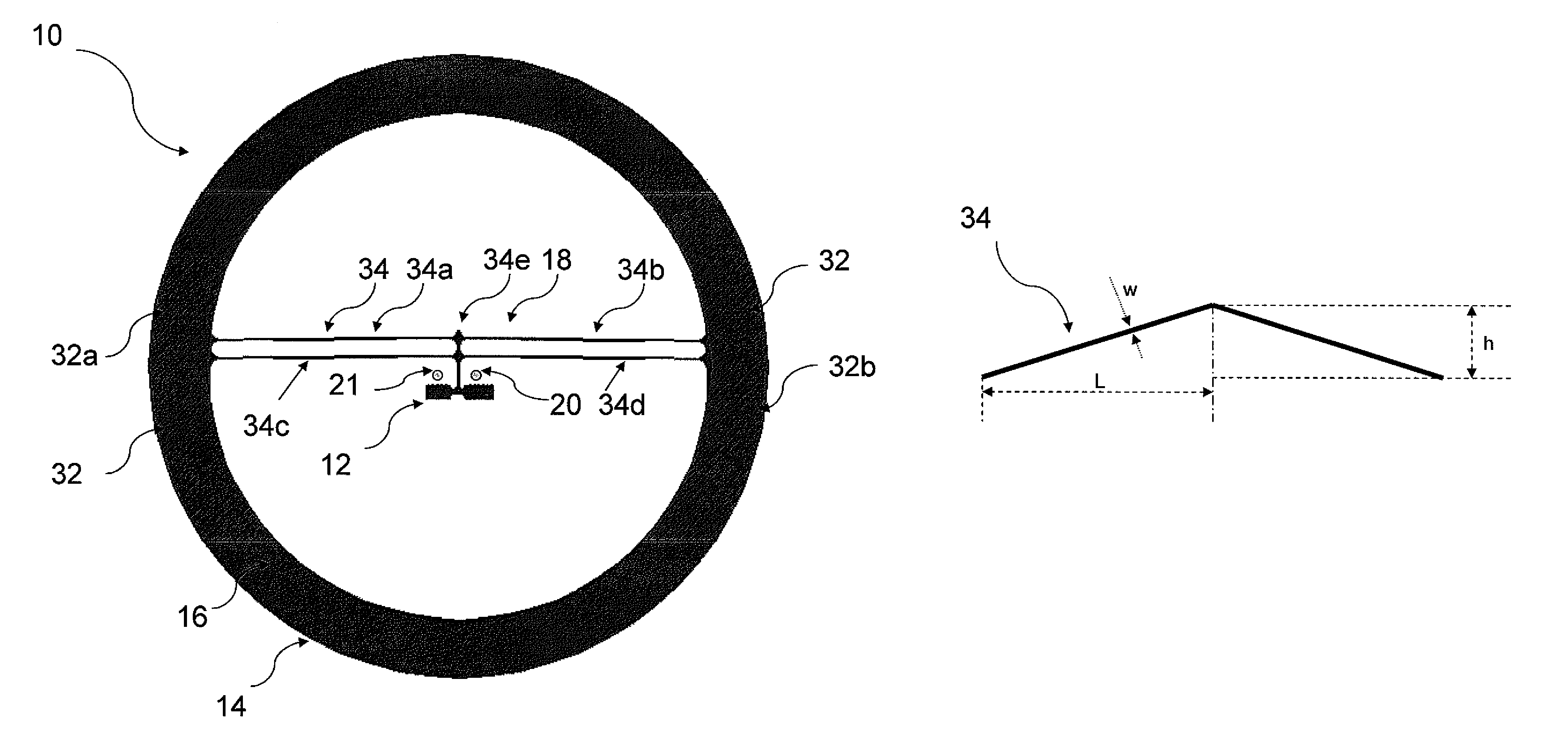
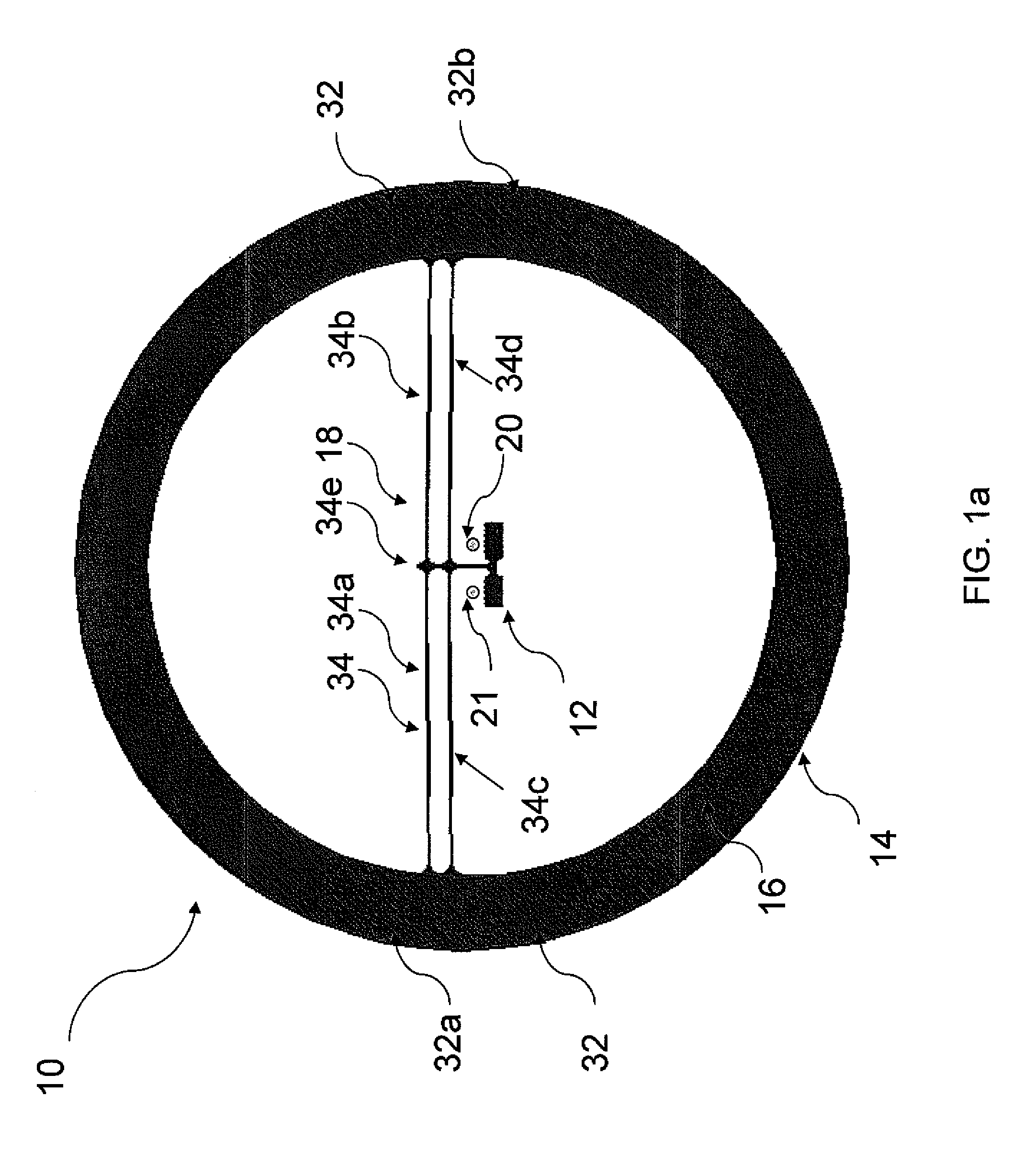
[0029]FIG. 1a illustrates a schematic view of an embodiment of a MEMS variable optical attenuator 10 in which an optical shutter 12 is utilized in accordance with one embodiment of these teachings.

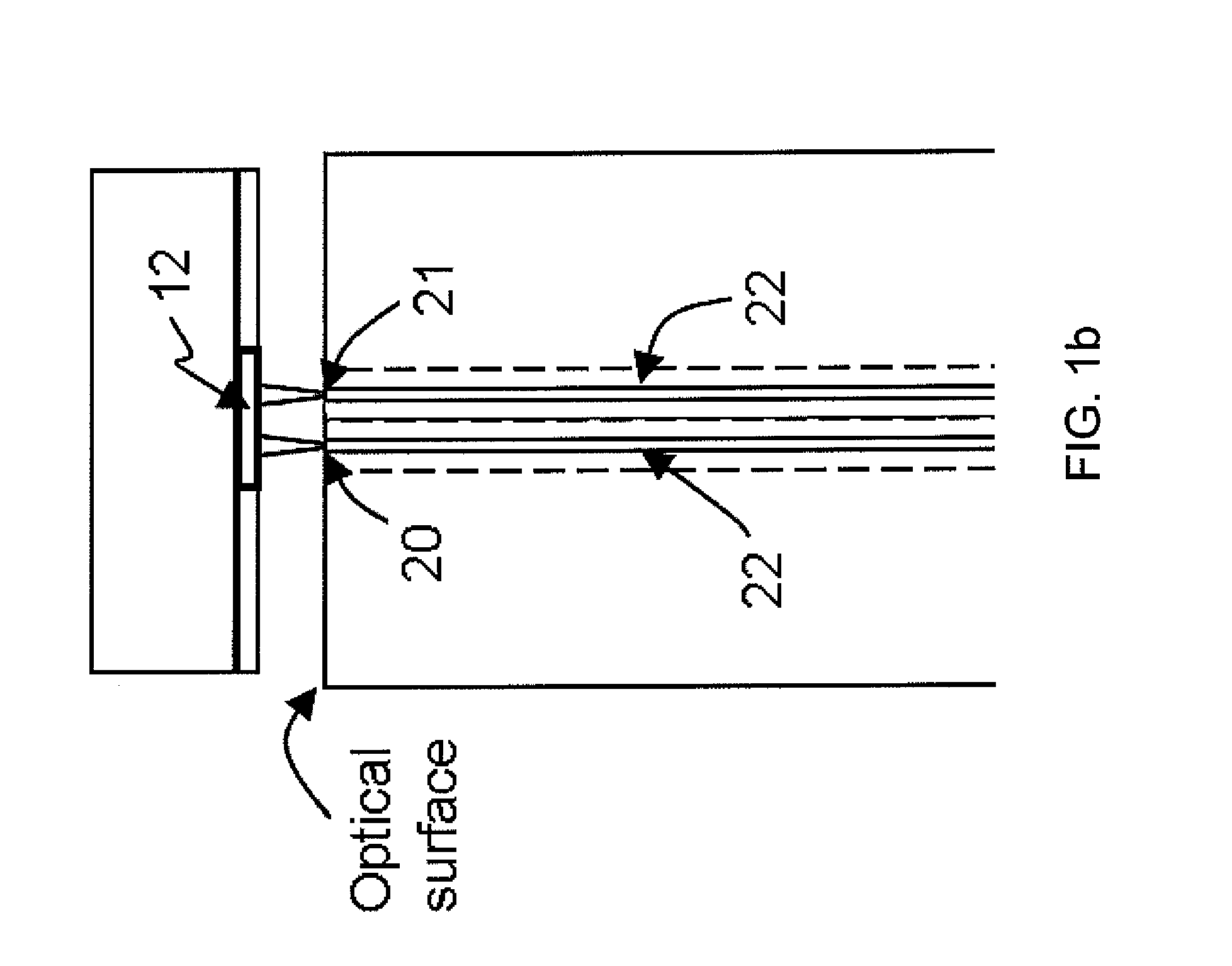
[0030]More specifically, the MEMS variable optical attenuator (VOA) or VOA chip 10 includes a substrate 14 (embodiments in which the VOA chip is lifted from the substrate are also within the scope of these teachings) having a planar surface frame 16, a micro-electric actuator 18 arranged on the planar surface 16 of the substrate 14, and optically aligned with each other while being arranged against the planar surface 16, an optical shutter 12 movable to a predetermined position over the receiving optical port 20 or the transmitting optical port 21 (in one instance, as shown in FIG. 1b, the op...


PUM

PropertyMeasurementUnit
temperatureaaaaaaaaaa
areaaaaaaaaaaa
widthaaaaaaaaaa

Abstract

A MEMS variable optical attenuator (VOA) chip includes a frame having a planar surface, a micro-electric actuator with a movable optical shutter arranged with respect to the planar surface of the frame, where the VOA is actuated by thermal expansion. The micro-electric actuator comprises semiconductor conductors (“wires”) that can be moved, upon applying an electrical current, by thermal expansion. In one embodiment, the MEMS VOA chip is configured in a multiple wire arrangement that restricts the shutter movement in a plane.

Description

BACKGROUND[0001]A variable optical attenuator (VOA) is an electro-optical component capable of attenuating an optical power by a varied amount of attenuation based on a user's requirements by applying an electrical control signal. Variable optical attenuators are widely used to control or regulate optical power levels in optical telecommunication systems. For example, an optical attenuator is needed in optical telecommunication network laser sources to regulate an output optical power. In an other example, an optical attenuator is needed in laser detector when an optical signal with an excessive power level, that is, greater than a predetermined power level, is received. In a further example, an optical attenuator is needed to balance the optical power level among multiple channels in the EDFA (Erbium-Doped Fiber Amplifier) module.[0002]Variable optical attenuators have been produced by various methods, including electro-optical polarization rotation, waveguide index change, bulk me...

Claims


Application Information

Patent Timeline
Patent Type & Authority Patents(United States)
IPC IPC(8): G02B6/00
CPCG02B6/00B23P11/00G02B6/266G02B26/02G02B6/3594Y10T29/49826
Inventor HE, YIYIN, LUZHONGZHONG, GUIXIONGYAN, JUNZHAO, JING
Owner AGILTRON
Why Eureka
Try Eureka