Semiconductor device

a technology of semiconductor elements and semiconductors, applied in the direction of semiconductor devices, semiconductor/solid-state device testing/measurement, semiconductor/solid-state device details, etc., can solve the problems of easy short-circuit defect, easy short-circuit defect, short-circuit defect, etc., to maximize the function of the semiconductor element and prevent breakage

Active Publication Date: 2014-04-01
RENESAS ELECTRONICS CORP
View PDF9 Cites 3 Cited by
  • Summary
  • Abstract
  • Description
  • Claims
  • Application Information

AI Technical Summary

Benefits of technology

[0004]The semiconductor device is composed of a semiconductor chip on which a semiconductor element such as a MOSFET (Metal Oxide Semiconductor Field Effect Transistor) and a multilayer interconnection are formed, and a package formed so as to cover the semiconductor chip. The package has (1) a function of electrically connecting the semiconductor element formed on the semiconductor chip and an external circuit to each other and (2) a function of protecting the semiconductor chip from external environment such as moisture or temperature and preventing breakage due to vibrations or an impact or characteristic deterioration of the semiconductor chip. Further, the package also has (3) a function of facilitating handling of the semiconductor chip, (4) a function of radiating heat generated during operation of the semiconductor chip to maximize the function of the semiconductor element, and the like.
[0007]However, in the current connection structure using a wire via a ball for connection between a pad and a terminal, the inventors of the present invention have newly found that the problems described below become apparent according to rising of the temperature of the semiconductor device. That is, in the current connection structure, a material forming the ball becomes easy to diffuse in a material forming the pad according to rising of the temperature, which results in formation of an alloy layer of the material forming the ball and the material forming the pad in the pad. When the temperature of the semiconductor device is retained at a high temperature, the alloy layer grows to break through an insulating film (glass coat) provided between pads for insulation so that such an event that the alloy layer reaches an adjacent pad or alloy layers which have grown from respective pads adjacent to each other to come in contact with each other occurs. In this case, the pads adjacent to each other are electrically connected to each other, which results in short-circuit defect. Especially, in recent years, the high functionality and size reduction of the semiconductor device are promoted, and a distance between pads adjacent to each other becomes short according to the promotion, which results in such a situation that short-circuit defect easily occurs. That is, there is the situation where short-circuit defect occurs easily due to a joint result of the operation guarantee at a high temperature and narrowing of a pitch between pads.
[0008]A preferred aim of the present invention is to provide technique capable of achieving reliability improvement of a semiconductor device even when temperature rising of the operation guarantee temperature of the semiconductor device has been performed.
[0013]According to the embodiment, even if temperature rising of the operation guarantee temperature of the semiconductor device is performed, reliability improvement of the semiconductor device can be achieved.

Problems solved by technology

In this case, the pads adjacent to each other are electrically connected to each other, which results in short-circuit defect.
Especially, in recent years, the high functionality and size reduction of the semiconductor device are promoted, and a distance between pads adjacent to each other becomes short according to the promotion, which results in such a situation that short-circuit defect easily occurs.
That is, there is the situation where short-circuit defect occurs easily due to a joint result of the operation guarantee at a high temperature and narrowing of a pitch between pads.

Method used


Image

  • Semiconductor device
  • Semiconductor device
  • Semiconductor device

Examples


first embodiment

[0063]

[0064]As a package structure of a semiconductor device, there are various kinds of ones such as, for example, a BGA (Ball Grid Array) package or a QFP (Quad Flat Package) package. The technical idea of the present invention can be adopted to these packages, and a configuration example of a semiconductor device formed in the BGA package and a configuration example of a semiconductor device formed in the QFP package will be described below.

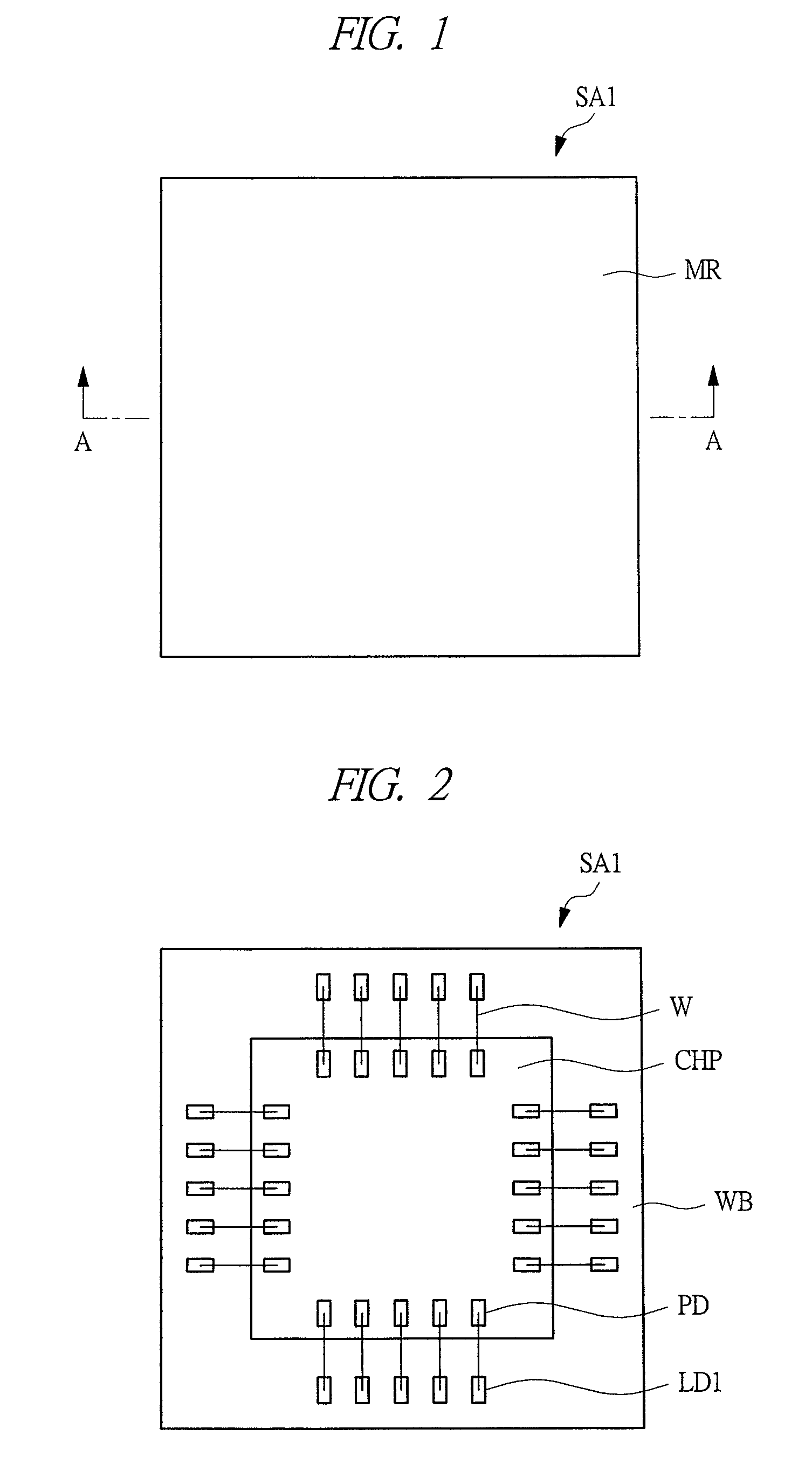
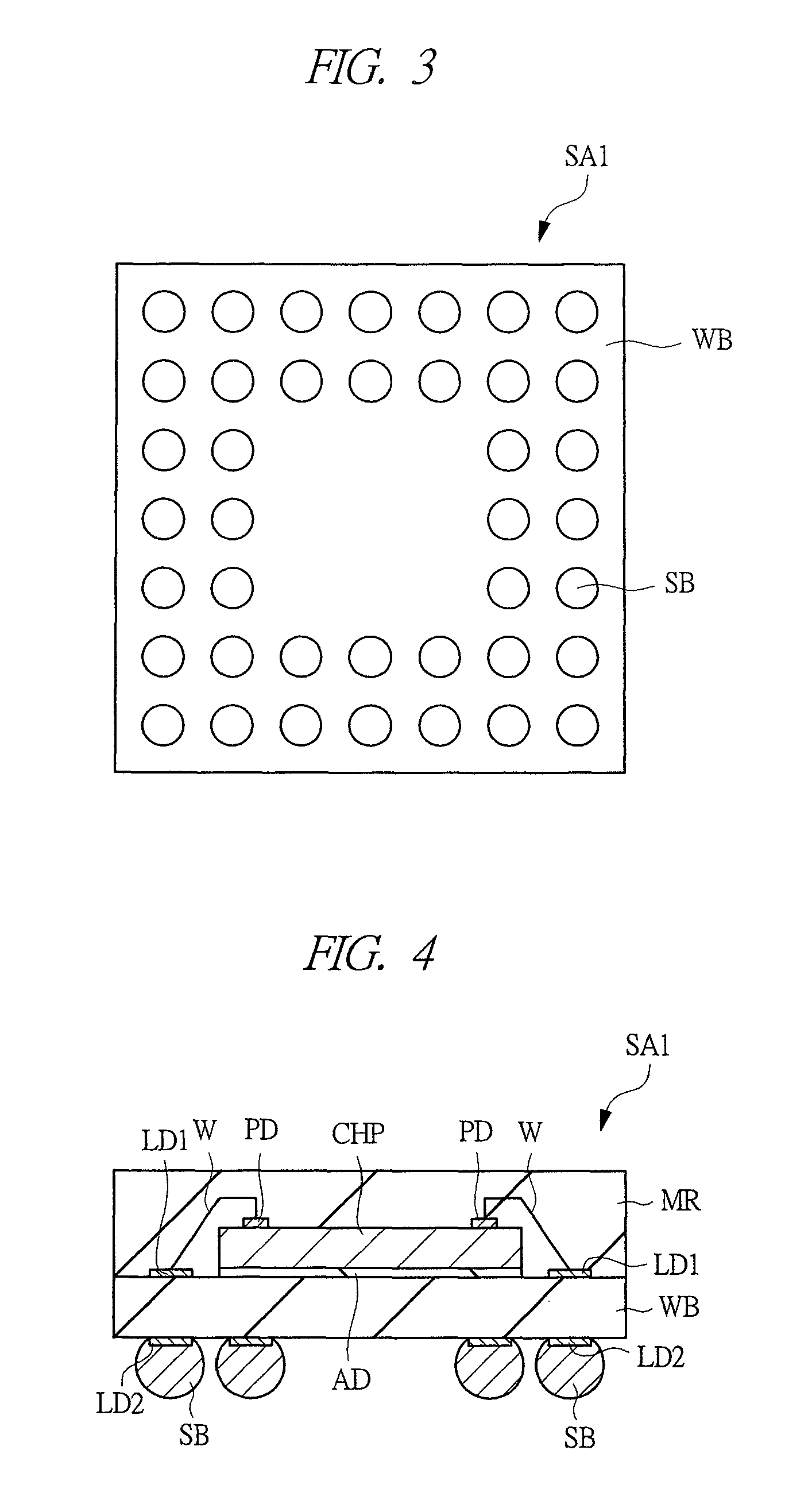
[0065]First, the configuration example of a semiconductor device formed in the BGA package will be described with reference to the drawings. FIG. 1 is a plan view of a semiconductor device SA1 formed in a BGA package as viewed from above. As illustrated in FIG. 1, the semiconductor device SA1 according to the present embodiment is formed in a rectangular shape, and an upper surface of the semiconductor device SA1 is covered with a resin (sealing body) MR.

[0066]Subsequently, FIG. 2 is a diagram of the semiconductor device SA1 illustrating the r...

second embodiment

[0143]

[0144]FIG. 22 is a cross-sectional view illustrating a connection structure between a pad and a wire according to a second embodiment. Since the connection structure according to the second embodiment illustrated in FIG. 22 is substantially similar to the connection structure in the first embodiment illustrated in FIG. 12, different points between the embodiments will be mainly described. In FIG. 22, step portions DIF1 are formed on end portions of a pad PD1 in the second embodiment. Similarly, step portions DIF2 are also formed on end portions of a pad PD2, and step portions DIF3 are also formed on end portions of a pad PD3. A trench is formed by the step portion DIF1 and the step portion DIF2, and a gap portion is formed on a bottom portion of the trench. At this time, a glass coat GC1 is formed so as to be embedded into the inside of the gap portion between the pad PD1 and the pad PD2 and extend on the bottom portion of the trench. That is, the glass coat GC1 is formed on t...

third embodiment

[0154]

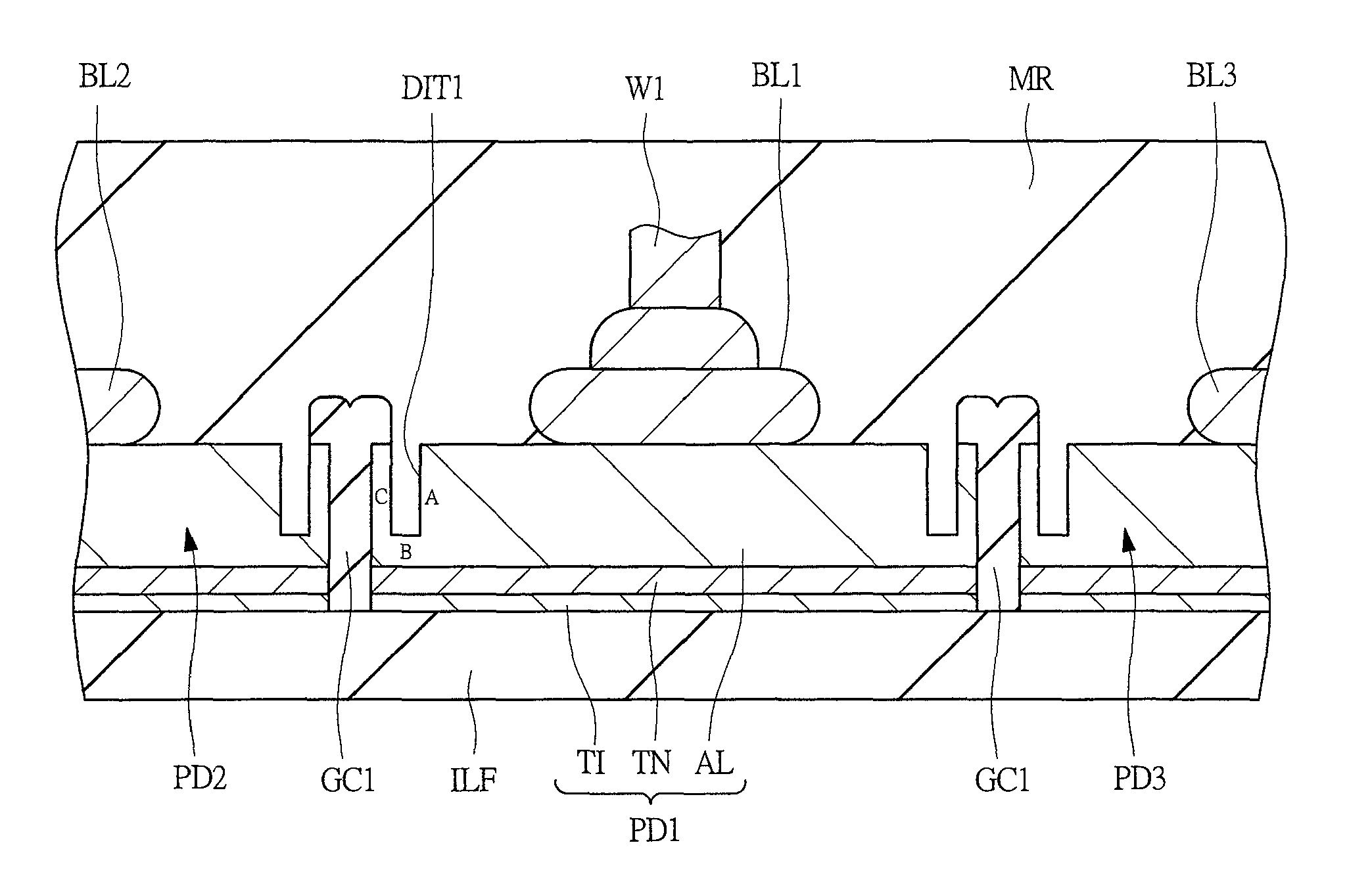
[0155]FIG. 26 is a cross-sectional view illustrating a connection structure between a pad and a wire according to a third embodiment. Since the connection structure in the third embodiment illustrated in FIG. 26 has a configuration substantially similar to that in the first embodiment illustrated in FIG. 12, different points between the connection structures will be mainly described. In FIG. 26, a plurality of pads PD1 to PD3 are each formed of a stacked film composed of a titanium film TI, a titanium nitride film TN, and an aluminum film AL. Here, in the present specification, a combined film of the titanium film TI and the titanium nitride film TN is called “lower layer film”, while the aluminum film AL is called “upper layer film”. In this case, in FIG. 26, a gap portion CE1 is formed between the lower layer film of the pad PD1 and the lower layer film of the pad PD2, and a glass coat GC2 is formed on an upper surface of a portion of the lower layer film of the pad PD1 and ...


PUM

PropertyMeasurementUnit
temperatureaaaaaaaaaa

Abstract

Technique capable of achieving reliability improvement of a semiconductor device even if temperature rising of an operation guarantee temperature of the semiconductor device is performed is provided. Gap portions are provided among a plurality of pads, and a glass coat composed of, for example, a silicon oxide film or a silicon nitride film is embedded in the gap portions. The glass coat is provided in order to secure electrical insulation among the pads, and coats outer edge portions of the pads. Trenches are formed so as to be adjacent to regions, which are coated with the glass coat, of the outer edge portions of the pads.

Description

CROSS-REFERENCE TO RELATED APPLICATION[0001]The present application claims priority from Japanese Patent Application No. 2012-051546 filed on Mar. 8, 2012, the content of which is hereby incorporated by reference into this application.TECHNICAL FIELD OF THE INVENTION[0002]The present invention relates to a semiconductor device. The present invention particularly relates to technique effectively used in a semiconductor device which electrically connects a terminal formed to a wiring member and a semiconductor chip mounted on the wiring member to each other using a metal wire.BACKGROUND OF THE INVENTION[0003]Japanese Patent Application Laid-Open No. 2003-243443 (Patent Document 1) describes technique for providing a semiconductor device having a pad excellent in adhesiveness according to a simple manufacturing process. Specifically, the semiconductor device is provided with a pad for connection of a gold wire serving as a bonding wire. The pad is formed on a flat surface of an insulat...

Claims


Application Information

Patent Timeline
Patent Type & Authority Patents(United States)
IPC IPC(8): H01L23/48H01L23/52H01L29/40
CPCH01L2224/48463H01L2224/49431H01L24/06H01L2224/48624H01L2224/48227H01L23/16H01L2924/10329H01L2224/05553H01L2924/15311H01L2224/49175H01L2224/48247H01L2224/48095H01L2224/92247H01L2224/48091H01L2224/05551H01L23/562H01L22/32H01L24/45H01L23/4952H01L2224/05624H01L2224/45144H01L2924/10253H01L2224/32225H01L2224/04042H01L24/49H01L2224/02166H01L24/48H01L2224/73265H01L24/32H01L24/73H01L24/46H01L2224/0612H01L24/05H01L23/3142H01L24/09H01L2223/54406H01L2223/54486H01L2224/05124H01L2224/05554H01L2924/07802H01L2924/1305H01L2924/1306H01L2924/13091H01L23/535H01L2224/42H01L2924/12042H01L2924/181H01L2924/00012H01L2924/00014H01L2924/00H01L23/488H01L23/49
Inventor SHIN, SHIKOSAITO, TAKAYUKIHORIBE, HIROSHI
Owner RENESAS ELECTRONICS CORP
Why Eureka
Try Eureka