Solid-state imaging device, method of driving the device, and camera system with varied timing of sampling period for sampling a bias voltage during pixel readout

a solid-state imaging and bias voltage technology, applied in the field of solid-state imaging devices, can solve the problems of reducing the image quality of the image, affecting the image quality, so as to prevent noise and reduce the image quality

Inactive Publication Date: 2014-04-01
SONY SEMICON SOLUTIONS CORP
View PDF13 Cites 14 Cited by
  • Summary
  • Abstract
  • Description
  • Claims
  • Application Information

AI Technical Summary

Benefits of technology

[0049]According to the embodiments of the invention, it is possible to prevent noise which can degrade image quality, e.g., circuit noise generated by a bias voltage generating circuit and external noise coming from outside a device from entering a column processing system without adding an external capacity.

Problems solved by technology

As a result, the amount of a pixel signal becomes small relative to the amount of circuit noise.
Then, internal circuit noise of such a device and noise entering the device from outside have non-negligible influence on image quality.
At this time, circuit noise generated in the internal voltage generating circuit 8 and external noise coming from outside the device can enter the column circuit to degrade image quality.

Method used


Image

  • Solid-state imaging device, method of driving the device, and camera system with varied timing of sampling period for sampling a bias voltage during pixel readout
  • Solid-state imaging device, method of driving the device, and camera system with varied timing of sampling period for sampling a bias voltage during pixel readout
  • Solid-state imaging device, method of driving the device, and camera system with varied timing of sampling period for sampling a bias voltage during pixel readout

Examples


first embodiment

1. First Embodiment

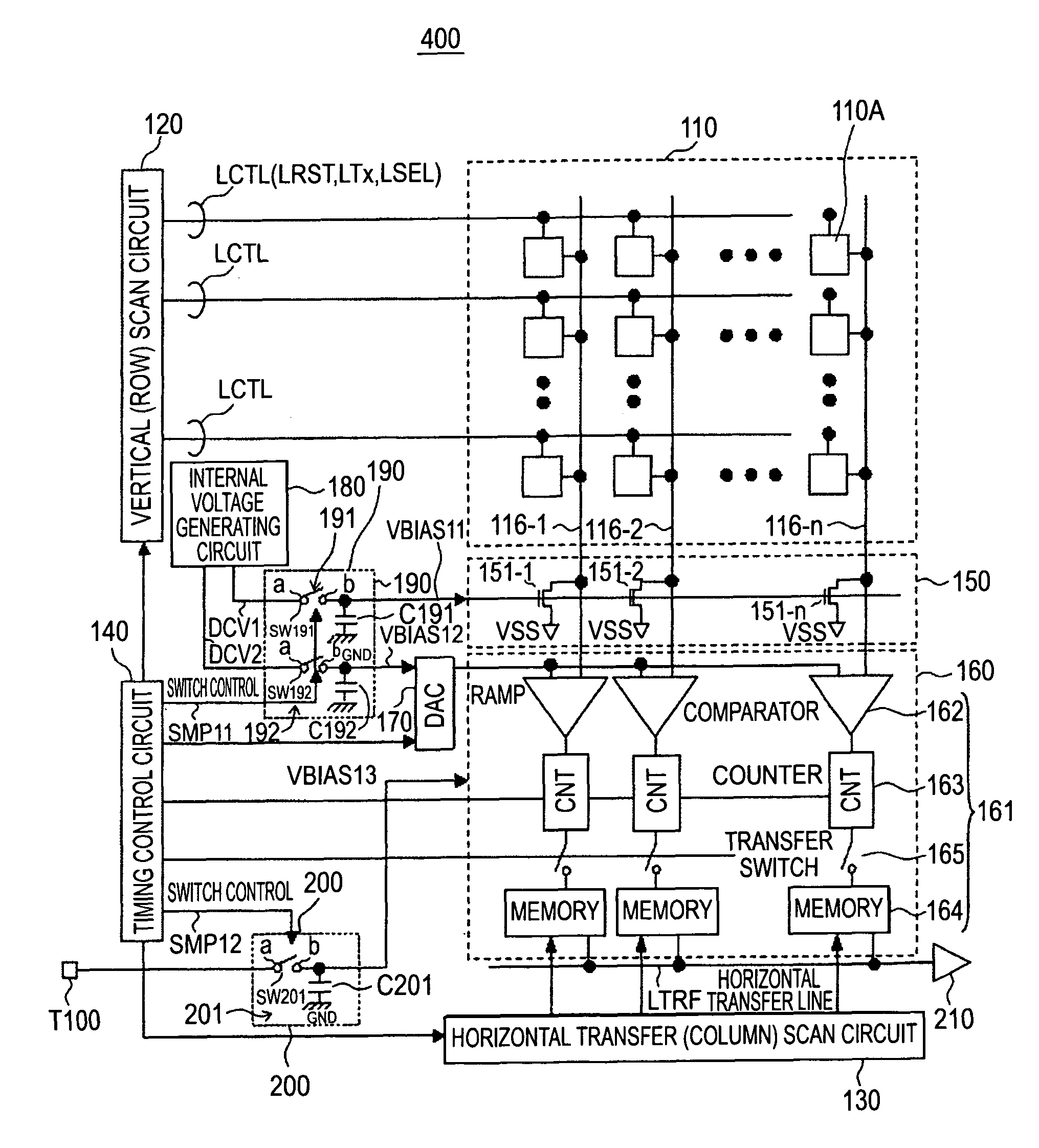
[0065]FIG. 3 is a block diagram showing an exemplary configuration of a solid-state imaging device (CMOS image sensor) having column-parallel ADCs incorporated therein according to an embodiment of the invention.

[0066]FIG. 4 is a block diagram which more specifically shows major parts of the solid-state imaging device (CMOS image sensor) having column-parallel ADCs incorporated therein according to the first embodiment shown in FIG. 3, the illustrated parts including a pixel section and a column circuit.

[Exemplary General Configuration of Solid-State Imaging Device]

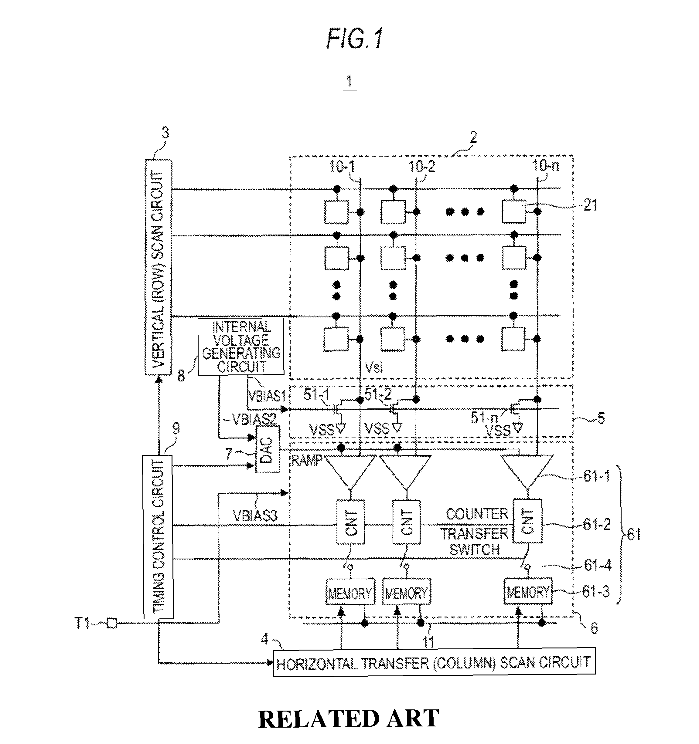
[0067]As shown in FIGS. 3 and 4, a solid-state imaging device 100 includes a pixel section 110, vertical scan circuit (row scan circuit) 120, a horizontal transfer scan circuit (column scan circuit) 130, and a timing control circuit 140.

[0068]Further, the solid-state imaging device 100 includes a load circuit 150 serving as a column circuit, a column-parallel processing section 160 which is a group of A...

second embodiment

2. Second Embodiment

[0233]FIG. 9 is a block diagram of a solid-state imaging device (CMOS image sensor) 100A having column-parallel ADCs in FIG. 3 according to a second embodiment of the invention, the diagram showing major parts of the device including a pixel section and a column circuit.

[0234]The solid-state imaging device 100A according to the second embodiment is different from the solid-state imaging device 100 according to the first embodiment in the following points.

[0235]In the solid-state imaging device 100 according to the first embodiment, the sample / hold portion 191 of the sample / hold circuit 190 is provided to supply a common bias voltage to the load circuit 150.

[0236]On the contrary, the solid-state imaging device 100A according to the second embodiment includes individual sample / hold portions 191A-1 to 191A-n provided in one-to-one association with load MOS transistors 151-1 to 151-n of a load circuit 150A.

[0237]The sample / hold portion 191A-1 includes a sampling swit...

third embodiment

3. Third Embodiment

[0266]FIG. 11 is a diagram showing an exemplary configuration of a camera system employing a solid-state imaging device according to a third embodiment of the invention.

[0267]As shown in FIG. 11, a camera system 400 includes an imaging device 410 which may be a solid-state imaging device 100 or 100A according to the above-described embodiments.

[0268]The camera system 400 includes an optical system for guiding incident light to a pixel region of the imaging device 410 (for forming an image of an object). For example, the optical system may be a lens 420 which forms an image of incident light (image light) on an imaging surface.

[0269]Further, the camera system 400 includes a driving circuit (DRV) 430 for driving the imaging device 410 and a signal processing circuit (PRC) 440 for processing signals output from the imaging device 410.

[0270]The driving circuit 430 includes a timing generator (not shown) generating various timing signals including a start pulse and a c...


PUM


Abstract

A solid-state imaging device includes: a pixel section formed by pixels performing photoelectric conversion arranged in a matrix; a pixel signal readout section capable of column-parallel processing including an A / D conversion function for reading out a pixel signal from the pixel section and performing analog-digital conversion of the signal, the pixels being read in groups; a voltage sampling section sampling a bias voltage generated by an internal or external voltage generating circuit for a period in accordance with a control signal and supplying the sampled bias voltage to the pixel signal readout section; and a control section controlling the signal readout operation of the pixel signal readout section and the voltage sampling operation of the voltage sampling section. The pixel signal readout section includes a functional portion. The control section exercises control such that the voltage sampling operation is performed in a period other than at least either of a period in which an analog signal is read out or in which A / D conversion is carried out.

Description

BACKGROUND OF THE INVENTION[0001]1. Field of the Invention[0002]The present invention relates to a solid-state imaging device from which data is read out on a column-parallel basis, a method of driving the device, and a camera system having the device.[0003]2. Description of the Related Art[0004]A CMOS image sensor can be manufactured using manufacturing processes similar to those used for common CMOS integrated circuits. A CMOS image sensor can be driven by a single power source and can be consolidated with analog circuits and logic circuits manufactured using CMOS processes into a single chip.[0005]Thus, CMOS image sensors have a multiplicity of significant advantages including the fact that they can be implemented in combination with a small number of peripheral ICs.[0006]It is the main trend in the related art to use one-channel (ch) output type CCD output circuits utilizing an FD amplifier having a floating diffusion (FD) layer.[0007]On the contrary, CMOS image sensors include ...

Claims


Application Information

Patent Timeline
Patent Type & Authority Patents(United States)
IPC IPC(8): H04N5/335H04N3/14
CPCH04N5/335H04N5/378H04N5/374H04N25/00H04N25/76H04N25/75
Inventor TOYAMA, TAKAYUKIIWAKI, HIROYUKI
Owner SONY SEMICON SOLUTIONS CORP
Why Eureka
Try Eureka