Solar cell fabrication with faceting and ion implantation
What is AI technical title?
AI technical title is built by Patsnap AI team. It summarizes the technical point description of the patent document.
a technology of solar cells and ion implantation, applied in the field of solar cell fabrication, can solve the problems of limited solar cell efficiency, excess un, and diffusion techniques used to form a conventional profile that are not optimal for the formation of selective doping regions
Active Publication Date: 2014-04-15
INTEVAC
View PDF390 Cites 23 Cited by
Summary
Abstract
Description
Claims
Application Information
AI Technical Summary
This helps you quickly interpret patents by identifying the three key elements:
Problems solved by technology
Method used
Benefits of technology
Benefits of technology
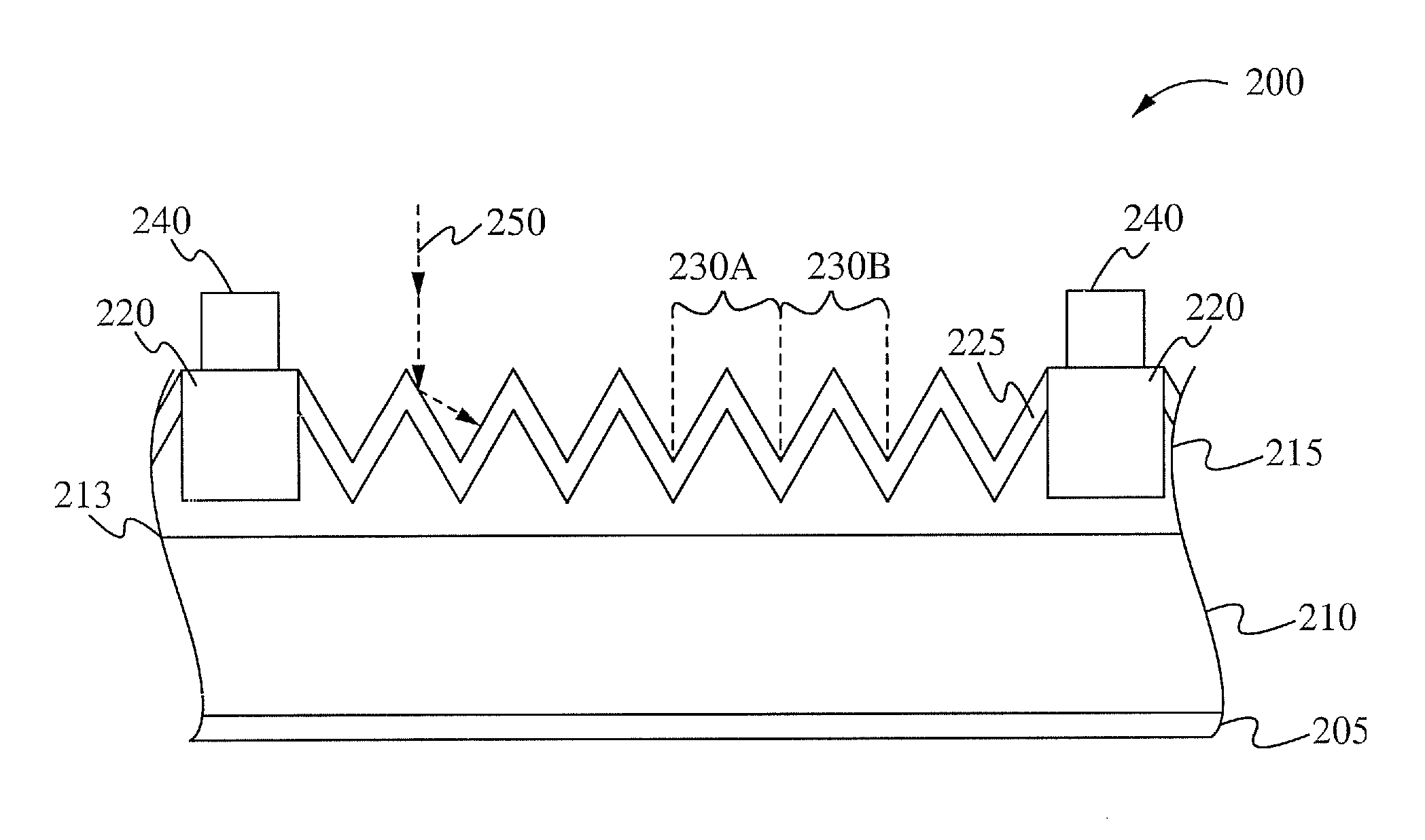
[0012]Preferably, each of the textured regions includes multiple textured elements, such as pyramidal elements having <111> planes, dome-shaped elements, or any other undulating (rising and falling) structures that reduce the amount of light reflected from the photo-receptive regions.
Problems solved by technology
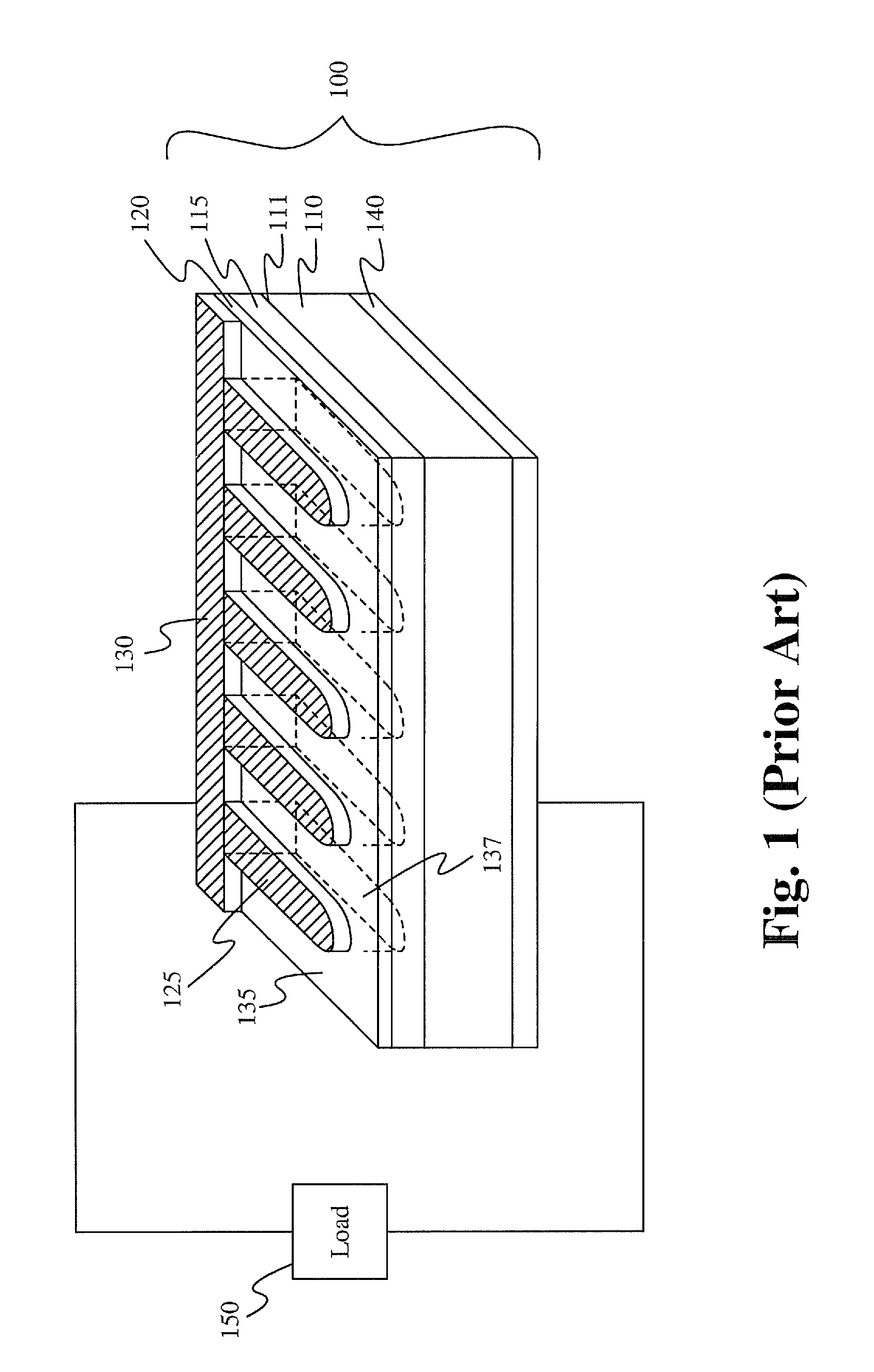
The efficiency of solar cells is limited in part by ohmic losses, which are affected by the dopant diffusion and contact screen printing used to fabricate the solar cells.
First, producing this profile results in excess un-activated dopants near the top surface, as the dopants are driven into the bulk of the substrate 100. This effect leads to varying levels of light absorption, the creation of electron-hole pairs, and unwanted recombination of electron-hole pairs. This is known as “dead layer,” in which blue light is not absorbed close to the top surface of the photo-receptive regions 135. Because of the high doping level near the surface, electron-hole pairs created in the dead layer quickly recombine before they can generate any current flow. Facetting, used to reduce the amount of light reflected from the solar cell before it can generate current.
Second, diffusion techniques used to form a conventional profile are not optimal for the formation of selective doping regions with a homogenous high resistivity photo-receptive region and low-resistance regions for gridlines, contact fingers, busbars, metal-silicon interfaces, and backside metallization.
Third, direct overlay of metal on the semiconductor can result in different work functions at the interface between the conductive fingers 125 and the emitter layer 115. To better match the work functions between a metal contact and the doped silicon, some prior art techniques melt the contacts 125 to form a silicide at the interface. While forming a silicide may help tailor the work functions, there are still undesirable ohmic losses and the potential of metal shunting.
Finally, lateral positioning of dopants across a substrate is becoming difficult as the line widths and wafer thicknesses are decreasing.
Present screen-printing techniques are ill equipped to fabricate devices with such small displacements.
Moreover, as wafers are getting ever thinner, vertical and batch diffusion and screen printing become extremely difficult.
Method used
Image
Click on the blue label to locate the original text in one second.
Reading with bidirectional positioning of images and text.
Examples
Embodiment Construction
[0037]Embodiments of the present invention are directed to methods of fabricating a solar cell by heavily doping its selective emitter region and more lightly doping its photo-receptive regions. In some embodiments, the selective emitter region and the photo-receptive regions are formed in the same processing step.
[0038]For the best performance of a solar cell, the photo-receptive regions are lightly doped to provide a homogeneous high sheet resistance. A more heavily doped region increases the chance of electron-hole recombination and thus decreases the efficiency of converting photons into electrical power. In accordance with embodiments, the n-doped layer of the photo-receptive regions of the solar cell is lightly doped to provide a sheet resistance of between 80 and 160 ohms per square, preferably 100 ohms per square, or an ion doping of around 1E+19 cm−3. Preferably, the gridlines, over which the conductive finger contacts are formed, are more heavily doped to couple the genera...
PUM
Abstract
Solar cells in accordance with the present invention have reduced ohmic losses. These cells include photo-receptive regions that are doped less densely than adjacent selective emitter regions. The photo-receptive regions contain multiple four-sided pyramids that decrease the amount of light lost to the solar cell by reflection. The smaller doping density in the photo-receptive regions results in less blue light that is lost by electron-hole recombination. The higher doping density in the selective emitter region allows for better contacts with the metallic grid coupled to the multiple emitter regions. Preferably, the selective emitter and photo-receptive regions are both implanted using a narrow ion beam containing the dopants.
Description
RELATED APPLICATIONS[0001]This application claims priority under 35 U.S.C. §119(e) of the U.S. provisional patent applications, Ser. No. 61 / 131,687, filed Jun. 11, 2008, and titled “Solar Cell Fabrication Using Implantation”; Ser. No. 61 / 131,688, filed Jun. 11, 2008, and titled “Application Specific Implant System for Use in Solar Cell Fabrications”; Ser. No. 61 / 131,698, filed Jun. 11, 2008, and titled “Formation of Solar Cell Selective Emitter Using Implant and Anneal Method”; Ser. No. 61 / 133,028, filed Jun. 24, 2008, and titled, “Solar Cell Fabrication with Faceting and Implantation”; and Ser. No. 61 / 210,545, filed Mar. 20, 2009, and titled “Advanced High Efficiency Crystalline Solar Cell Fabrications Method,” all of which are incorporated by reference in their entireties.FIELD OF THE INVENTION[0002]This invention relates to semiconductor devices and methods of fabricating them. More specifically, this invention relates to methods of fabricating solar cells with reduced ohmic loss...
Claims
Application Information
Patent Timeline
Application Date:The date an application was filed.
Publication Date:The date a patent or application was officially published.
First Publication Date:The earliest publication date of a patent with the same application number.
Issue Date:Publication date of the patent grant document.
PCT Entry Date:The Entry date of PCT National Phase.
Estimated Expiry Date:The statutory expiry date of a patent right according to the Patent Law, and it is the longest term of protection that the patent right can achieve without the termination of the patent right due to other reasons(Term extension factor has been taken into account ).
Invalid Date:Actual expiry date is based on effective date or publication date of legal transaction data of invalid patent.

