Color emitting device

a technology of emitting device and emitting device, which is applied in the direction of static indicating device, organic semiconductor device, instrument, etc., can solve the problems of low luminance of emitting device and impaired emission efficiency of organic el device, and achieve the effect of improving the luminance of the device itsel

Inactive Publication Date: 2006-07-20
IDEMITSU KOSAN CO LTD
View PDF5 Cites 37 Cited by
  • Summary
  • Abstract
  • Description
  • Claims
  • Application Information

AI Technical Summary

Benefits of technology

[0021] Since the light emitted from the color conversion member 21 is spatially isotropic, the light emitted from the color conversion member 21 contains a component “a” emitted toward the light-outcoupling side (indicated by the arrow in FIG. 9) of the color emitting device, and a component “b” emitted toward the organic EL device 10. In the top emission type color emitting device, the electrodes are generally formed by a metal exhibiting high reflecting properties or a metal compound thin film having a high refractive index. The second electrode 15 must transmit light. In this case, light b′ which is a part of the light component b is attenuated by multiple interference between the electrodes, and then disappears, so that the amount of light outcoupled from the device is decreased. As a result, the intensity of light emitted toward the viewer side (display surface) is decreased.
[0023] Based on the above findings, the inventors found that the intensity of light outcoupled from the device can be increased by increasing the reflectance of the emitting device for the peak wavelength of light emitted from the color conversion member. The inventors also found that the reflectance can be adjusted by the optical length between the first electrode and the second electrode forming the device, and the like. These findings have led to the completion of the invention.
[0062] The color emitting device according to the invention can improve the luminance of the device itself, since light (fluorescence or phosphorescence) converted by the color conversion member can efficiently be outcoupled to the outside of the device.

Problems solved by technology

However, when the film thickness is reduced to such a level, the organic emitting layer is extensively damaged when depositing the ITO electrode on the film, whereby the emission efficiency of the organic EL device is impaired.
However, when forming an emitting device using the color conversion member, since the intensity of light emitted from the emitting device is insufficient, the emitting device exhibits a low luminance.

Method used


Image

  • Color emitting device
  • Color emitting device
  • Color emitting device

Examples


first embodiment

[0104]FIG. 5 is a diagram showing a configuration of a color emitting device according to one embodiment of the invention.

[0105] The first embodiment is an example of a full color emitting device in which pixels respectively emitting light of blue, green, red of the three primary colors are separately arranged in a plane by using the technology according to the invention.

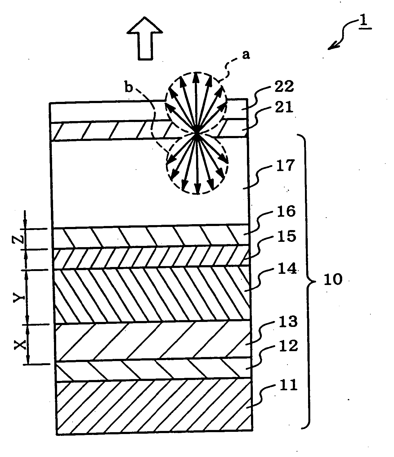
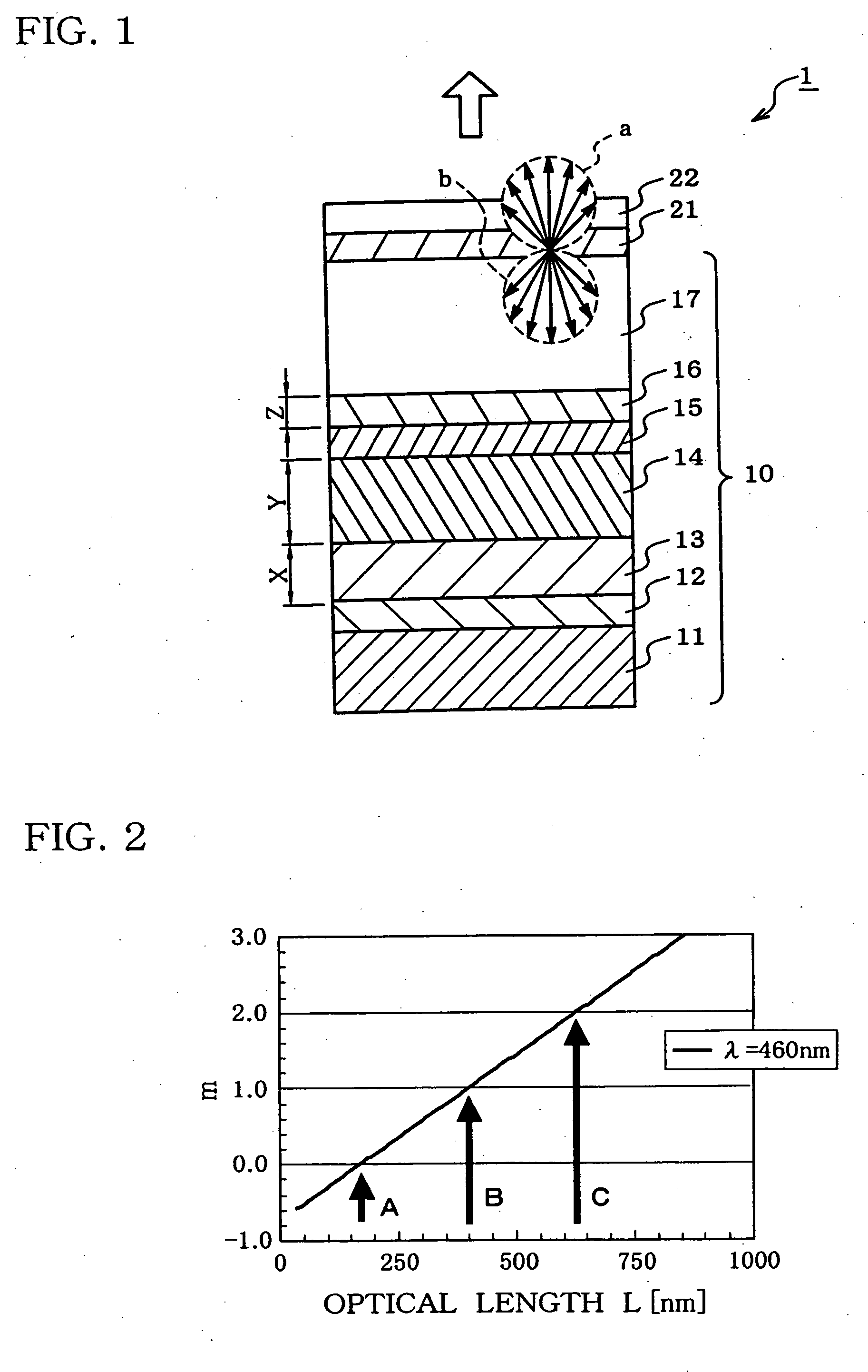
[0106] In a color emitting device 2, a blue pixel 101, a green pixel 102, and a red pixel 103 are formed on the supporting substrate 11. The arrow indicates the light-outcoupling direction.

[0107] The blue pixel 101 includes a first-organic EL device 41 and a blue color filter 51. The first organic EL device 41 has a configuration in which the first reflecting section 12, the organic emitting layer 14, the second reflecting section 15, the second transparent layer 16, and the gas barrier layer 17 are stacked in that order.

[0108] The green pixel 102 includes a second organic EL device 42 and a green color filter 5...

second embodiment

[0120] A second embodiment is another example of a full color emitting device in which emitting pixels respectively emitting light of blue, green, red of the three primary colors are separately arranged in a plane.

[0121] A full color emitting device 3 has the same configuration as the full color emitting device according to the first embodiment except that the green pixel 102 includes a green conversion member 32 formed between the second organic EL device 42 and the green color filter 52, and the first transparent layer 13 is formed instead of the third transparent layer 13′. The members of the full color emitting device 3 are the same as the corresponding members shown in FIG. 2.

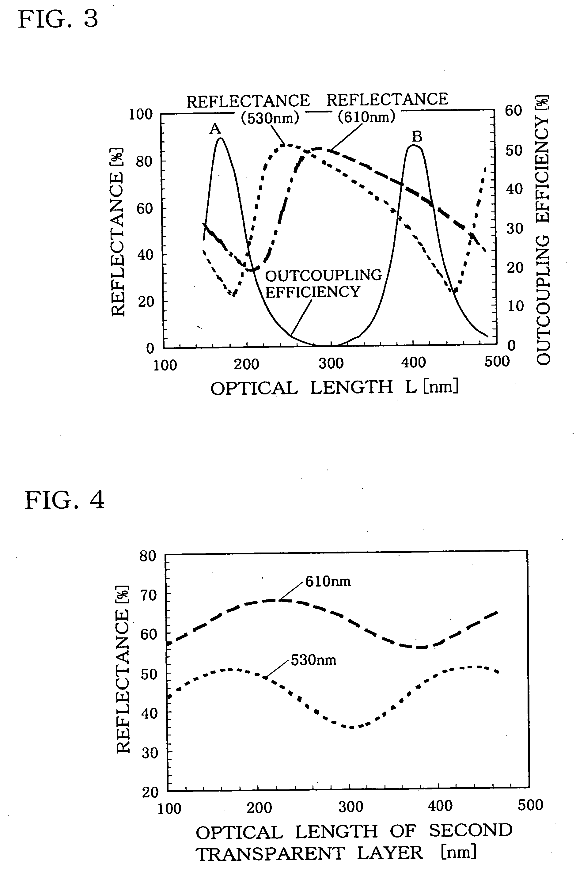
[0122] When the reflectance for the peak wavelength of light emitted from the green conversion member 32 and the reflectance for the peak wavelength of light emitted from the red conversion member 33 can be set at 50% or more, a configuration may be employed in which the green conversion member 33 and th...

example 1

1. Fabrication of Organic EL Device Substrate

[0279] Aluminum was deposited on a supporting substrate (75×25×1.1 mm) (0A2 glass manufactured by Nippon Electric Glass Co., Ltd.) by sputtering to a thickness of 300 nm. The aluminum film functions as a lower electrode and a first reflecting section.

[0280] ITO was deposited on the aluminum film by sputtering to a thickness of 130 nm. The ITO film functions as an electrode for injecting holes into an organic emitting layer, and also functions as a first transparent layer.

[0281] The substrate on which the lower electrode was formed was subjected to ultrasonic cleaning for five minutes in isopropyl alcohol, and then subjected to UV ozone cleaning for 30 minutes. The cleaned substrate was installed in a substrate holder of a vacuum deposition system.

[0282] A molybdenum heating boat was respectively charged in advance with a compound (HI) (hereinafter abbreviated as “HI film”) as a hole-injecting material, a compound (HT) (hereinafter ab...


PUM


Abstract

A color emitting device (1) comprising an emitting device (10) and a color conversion member (21) which absorbs light emitted from the emitting device (10) and emits light; the emitting device (10) including at least a first reflecting section (12) and a second reflecting section (15) provided in that order in a light-outcoupling direction, and an organic emitting layer (14) positioned between the first and second reflecting sections; the color conversion member (21) being positioned on a light-outcoupling side of the second reflecting section (15); and the emitting device (10) having a reflectance of 50% or more for a peak wavelength of the light emitted from the color conversion member (21).

Description

TECHNICAL FIELD [0001] The invention relates to a color emitting device. More particularly, the invention relates to a color emitting device suitable for a color display. BACKGROUND ART [0002] A color conversion method, in which light emitted from an emitting device is converted into light having a different wavelength by a color conversion member, is used for an organic electroluminescent (hereinafter abbreviated as “EL”) device, and is also useful for efficiently converting the color of light emitted from an emitting device (e.g. vacuum fluorescent display (VFD) or light emitting diode (LED)) or a liquid crystal display device. [0003] Organic EL color emitting devices using the color conversion method are roughly divided into a bottom emission type and a top emission type. [0004]FIG. 7 shows an example of a bottom emission type organic EL color emitting device. In the bottom emission type organic EL color emitting device, a color conversion member 70 and a thin film transistor (TF...

Claims


Application Information

Patent Timeline
Patent Type & Authority Applications(United States)
IPC IPC(8): G09G3/32
CPCH01L27/322H01L51/5036H01L51/5265H01L2251/5315H10K59/35H10K59/38H10K50/125H10K50/852H10K2102/3026H05B33/24H05B33/14H05B33/12
Inventor KUMA, HITOSHI
Owner IDEMITSU KOSAN CO LTD
Why Eureka
Try Eureka