Element array and footprint layout for element array

a technology of element array and footprint layout, applied in the field of multi-element array, can solve the problems of large capacitance value and severely limited the space such electronic components may occupy on the circuit board

Active Publication Date: 2014-04-15
KYOCERA AVX COMPONENTS CORP
View PDF7 Cites 7 Cited by
  • Summary
  • Abstract
  • Description
  • Claims
  • Application Information

AI Technical Summary

Benefits of technology

[0012]In accordance with yet additional aspects of certain embodiments of the present subject matter, an improved footprint layout is disclosed for providing for more efficient application and location of termination structures to an element array.
[0015]A further exemplary embodiment is directed to a multi-element varistor array. The multi-element varistor array includes a top dielectric layer, a bottom dielectric layer, and a plurality of stacked dielectric-electrode layers disposed between the dielectric layer and the bottom dielectric layer. The plurality of stacked dielectric-electrode layers are formed at least in part from zinc oxide. The plurality of stacked dielectric-electrode layers includes a first dielectric-electrode layer and a second dielectric-electrode layer. The first dielectric-electrode layer includes a plurality of electrodes forming a part of individual varistors for said varistor array. The second dielectric-electrode layer comprising a common electrode for said varistor array. During a voltage transient, current flows between one of the plurality of electrodes on the first dielectric-electrode layer and the common electrode, thereby providing transient voltage surge protection.

Problems solved by technology

For example, some applications require a large capacitance value, but are severely limited in the amount of space such electronic components may occupy on a circuit board.

Method used


Image

  • Element array and footprint layout for element array
  • Element array and footprint layout for element array
  • Element array and footprint layout for element array

Examples


example 1

[0058]In this example, a 1206 eight varistor array was constructed as shown and described above with reference to FIGS. 1-5. The varistor array included two top dielectric layers, thirty layers of alternating dielectric-conductor layers, and one bottom dielectric layer. Each dielectric layer was about 2.9 mils thick. With current at 1 A, the clamping voltage was about 44.68 V. The breakdown voltage was about 24.2 V at 1 mA. At 18 V the maximum leakage current was about 0.235 μA. The average capacitance was about 64.41 pF at 1 MHz and 0.5 V.

example 2

[0059]In this example, a 1206 eight varistor array was constructed as shown and described above with reference to FIGS. 1-5. The varistor array included seven top dielectric layers, twenty layers of alternating dielectric-conductor layers, and six bottom layers. Each dielectric layer was about 2.9 mils thick. With current at 1 A, the clamping voltage was about 48.52 V. The breakdown voltage was about 26.75 V at 1 mA. At 18V the maximum leakage current was about 0.034 μA. The average capacitance was about 45.56 pF at 1 MHz and 0.5 V.

example 3

[0060]In this example, a 1206 eight varistor array was constructed as shown and described above with reference to FIGS. 1-5. The varistor array included twelve top dielectric layers, ten layers of alternating dielectric-conductor layers, and eleven bottom layers. Each dielectric layer was about 2.9 mils thick. With current at 1 A, the clamping voltage was about 48.17 V. The breakdown voltage was about 25.04 V at 1 mA. At 18V the maximum leakage current was about 0.035 μA. The average capacitance was about 33.46 pF at 1 MHz and 0.5 V.

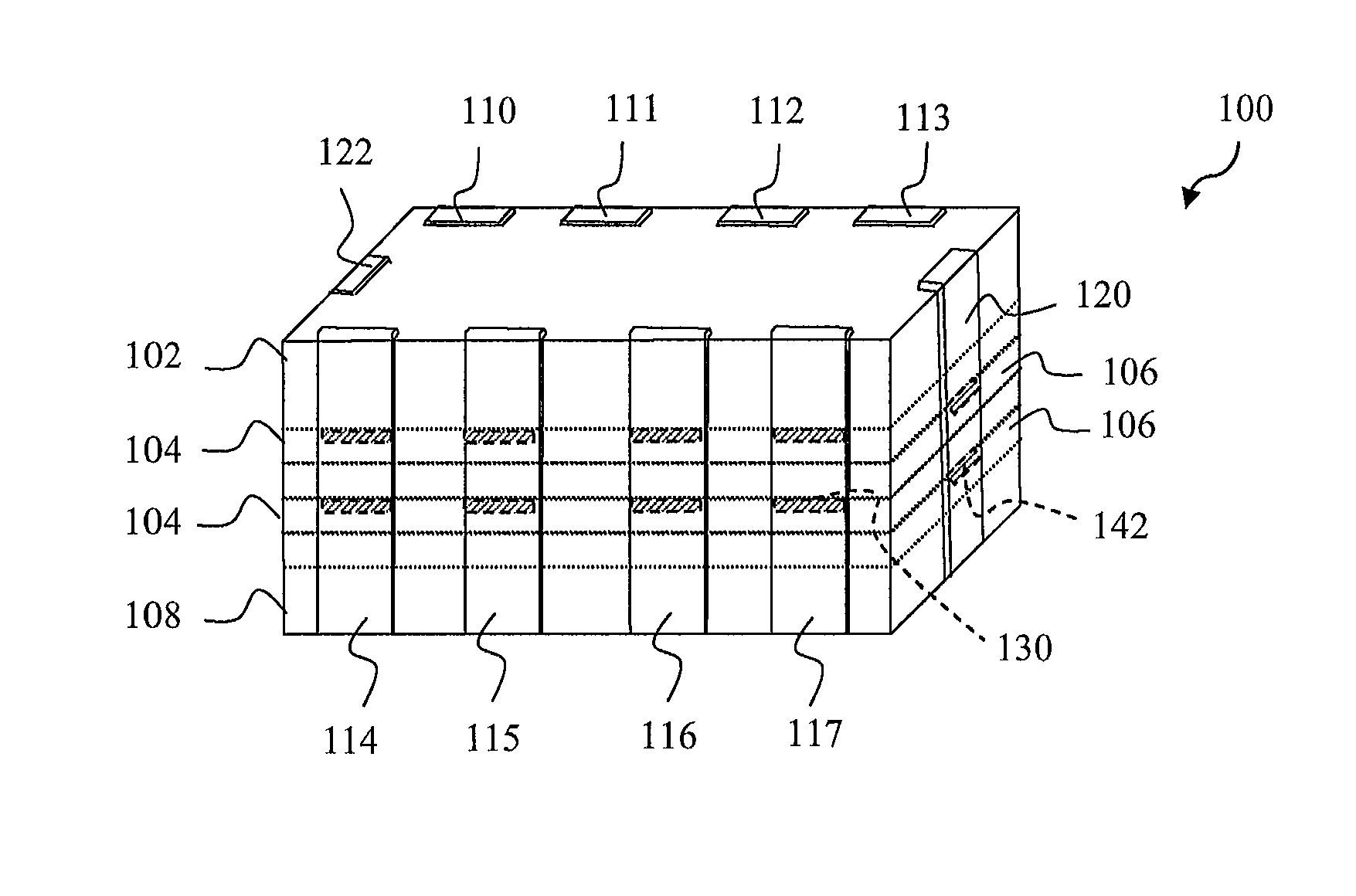
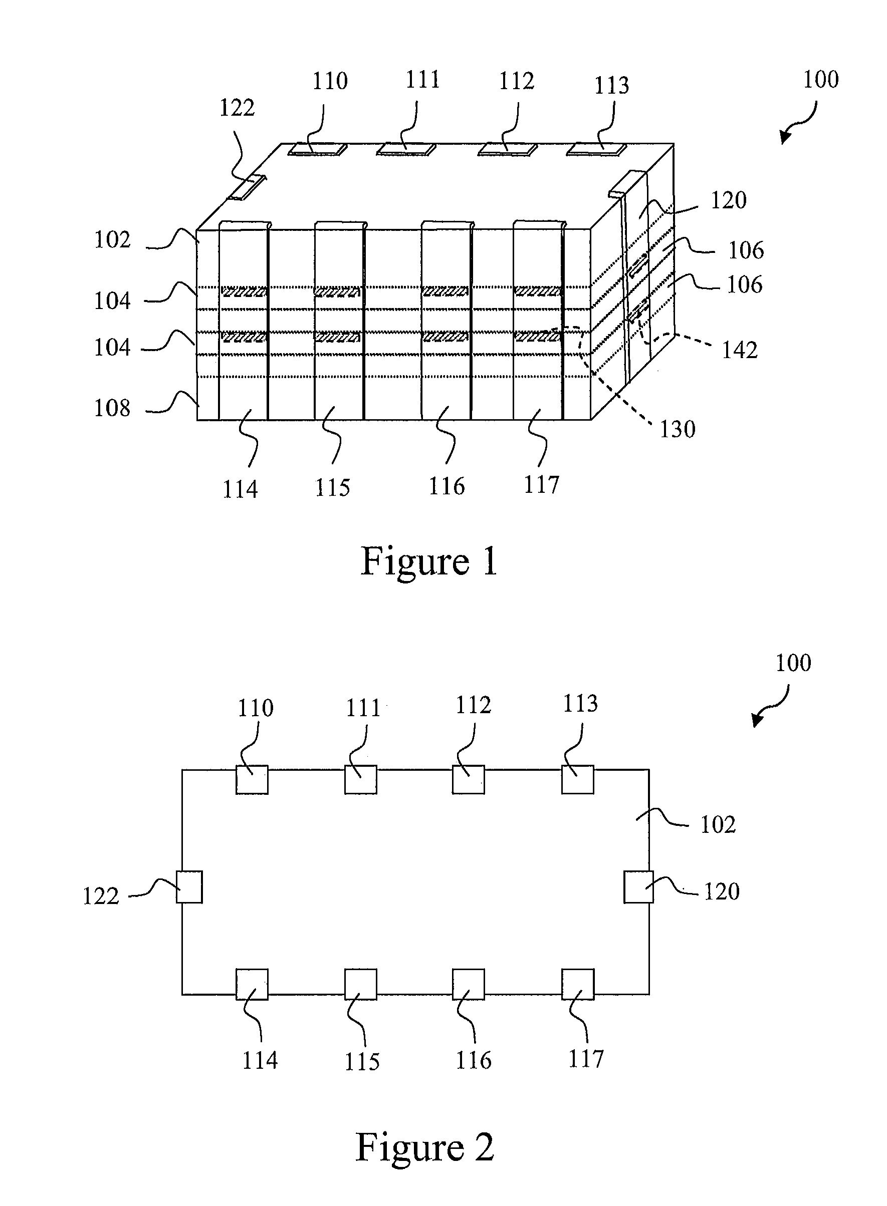
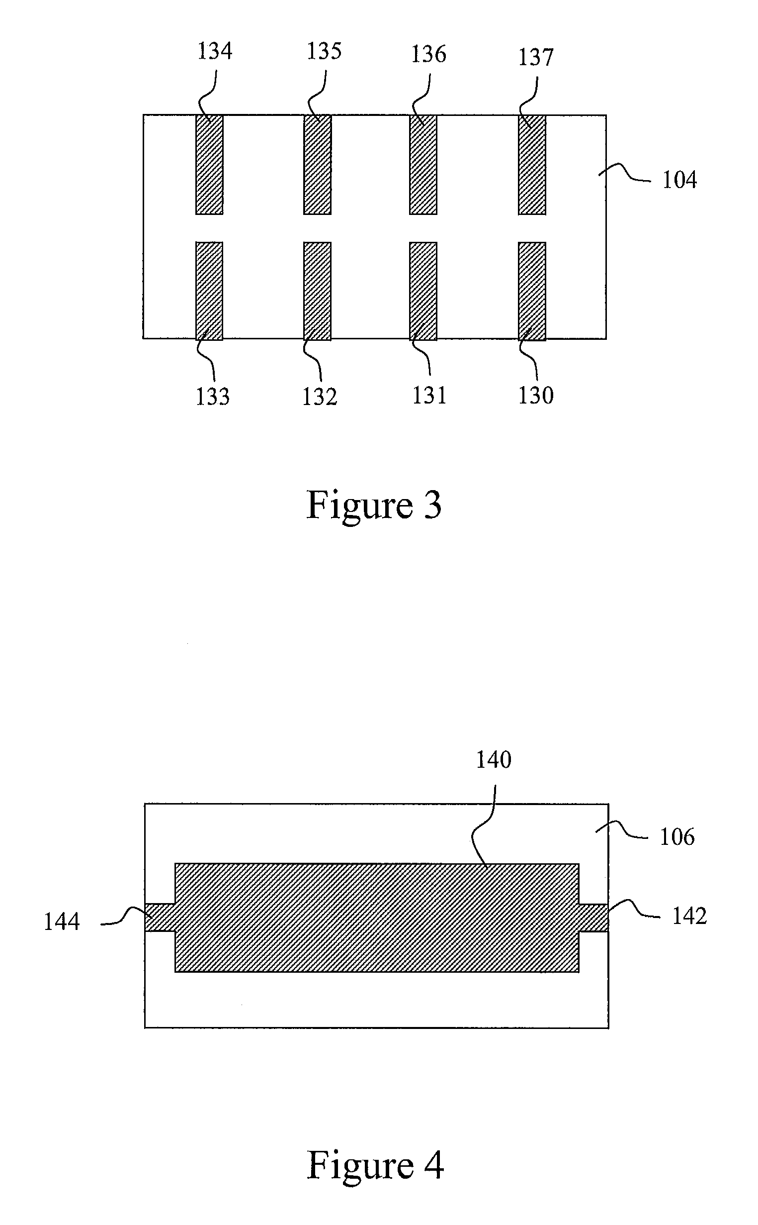
[0061]Referring now to FIGS. 6-17, another exemplary embodiment of the present disclosure is discussed in detail. FIG. 6 provides a perspective view of an exemplary element array 200 that can be mounted to a printed circuit board. FIG. 7 provides a top plan view of element array 200. Element array 200 can be a capacitor array, a varistor array, a resistor array, or other suitable array.

[0062]Element array 200 includes a plurality of generally planar diel...


PUM


Abstract

An element array and a footprint layout for an element array are disclosed. The element array can have a rectangular configuration defining two side surfaces and two end surfaces. The element array can include a plurality of stacked dielectric-electrode layers. One dielectric-electrode layer can include a plurality of element electrodes, such as eight element electrodes. Each of the plurality of element electrodes forms a part of an individual element for the element array. The element array device can further include a common electrode. The common electrode is used as part of each of the individual elements for the element array. The common electrode can include a lead for termination to one of the two end surfaces of the element array or, in a particular embodiment, to one of the two side surfaces of the element array.

Description

PRIORITY CLAIM[0001]The present application claims the benefit of priority of U.S. Provisional Patent Application Ser. No. 61 / 307,141, filed Feb. 23, 2010, which is incorporated herein by reference for all purposes.BACKGROUND OF THE INVENTION[0002]The present subject matter generally relates to electronic components adapted to be mounted on a circuit board and more particularly to a multi-element array, such as a capacitor array or a varistor array, and relates to a footprint layout for such multi-element array for use in a variety of applications.[0003]For some time, the design of various electronic components has been driven by a general industry trend toward miniaturization. In this regard, a need exists for ever smaller electronic components having exceptional operating characteristics. For example, some applications require a large capacitance value, but are severely limited in the amount of space such electronic components may occupy on a circuit board.[0004]Multilayer ceramic...

Claims


Application Information

Patent Timeline
Patent Type & Authority Patents(United States)
IPC IPC(8): H01G4/005H01G4/228H01G4/232H01G4/30
CPCH01C1/16H01G4/30H01G4/228H01G4/232H01G4/005H01C1/14H01C7/10H01G4/385
Inventor DEMCKO, RONALD S.CHENG, JEFFKIRK, MICHAEL
Owner KYOCERA AVX COMPONENTS CORP
Why Eureka
Try Eureka