Thermal interface material

a technology of thermal interface material and heat exchange path, which is applied in the field of thermal interface material, can solve the problems of microscopic unevenness, non-planarity between the mating surfaces, and the cooling of the power semiconductor device, and achieve excellent heat exchange path and add to the heat transfer capacity of the material

Inactive Publication Date: 2014-04-22
UNIV COLLEGE CORK NAT UNIV OF IRELAND CORK
View PDF17 Cites 1 Cited by
  • Summary
  • Abstract
  • Description
  • Claims
  • Application Information

AI Technical Summary

Benefits of technology

[0011]The aligned sub-micron wires give excellent heat transfer paths and the body may be chosen for the required degree of flexibility for conformity with the end-application devices with which it is in contact.
[0012]In one embodiment, the wires include nano-scale carbon particles aligned in the metal. This considerably adds to heat transfer capacity of the material.

Problems solved by technology

One of the main limitations in power semiconductor device cooling is the microscopic unevenness and non-planarity between the mating surfaces (chip and heat sink).

Method used


Image

  • Thermal interface material
  • Thermal interface material
  • Thermal interface material

Examples


Embodiment Construction

Brief Description of the Drawings

[0031]The invention will be more clearly understood from the following description of some embodiments thereof, given by way of example only with reference to the accompanying drawings in which:

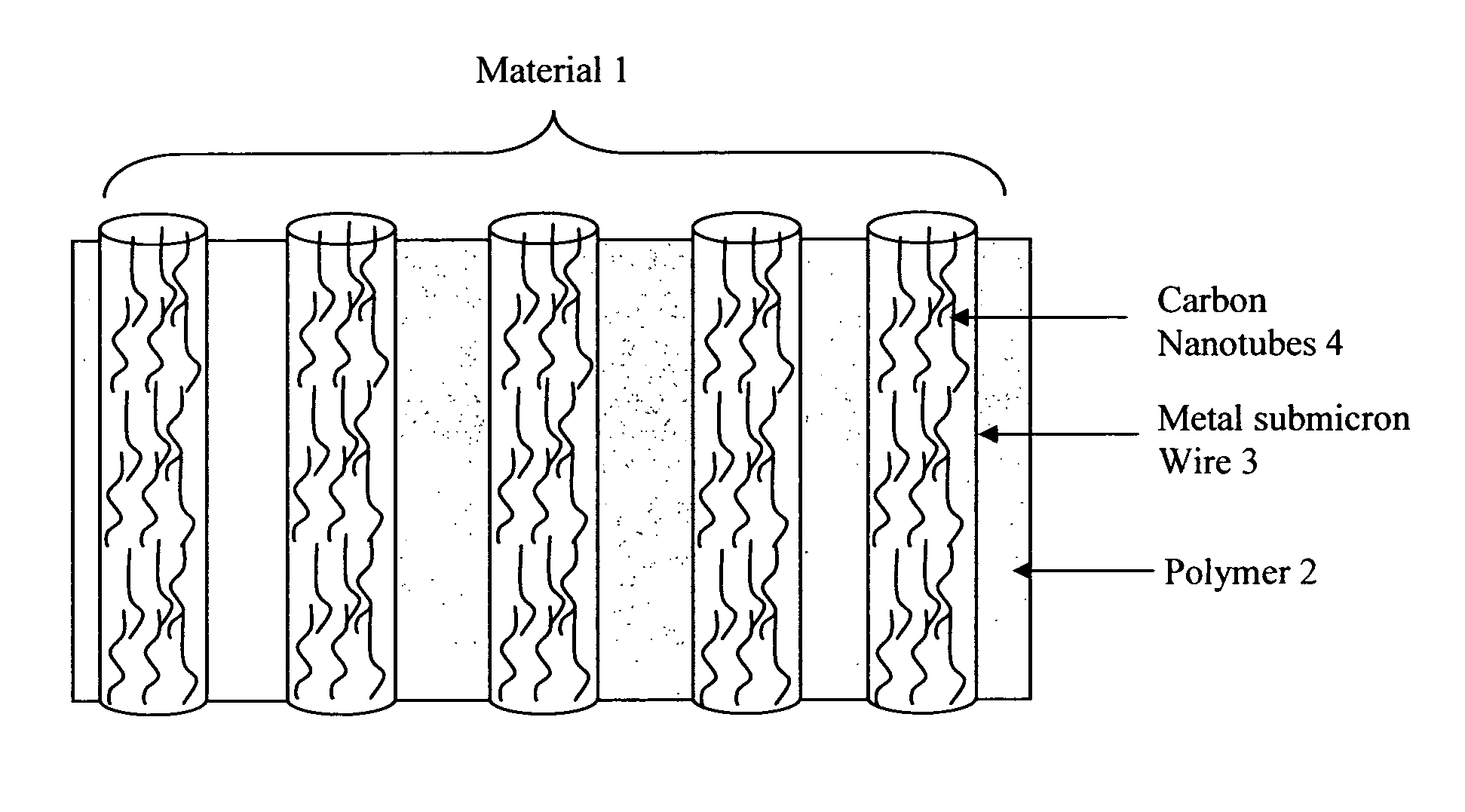
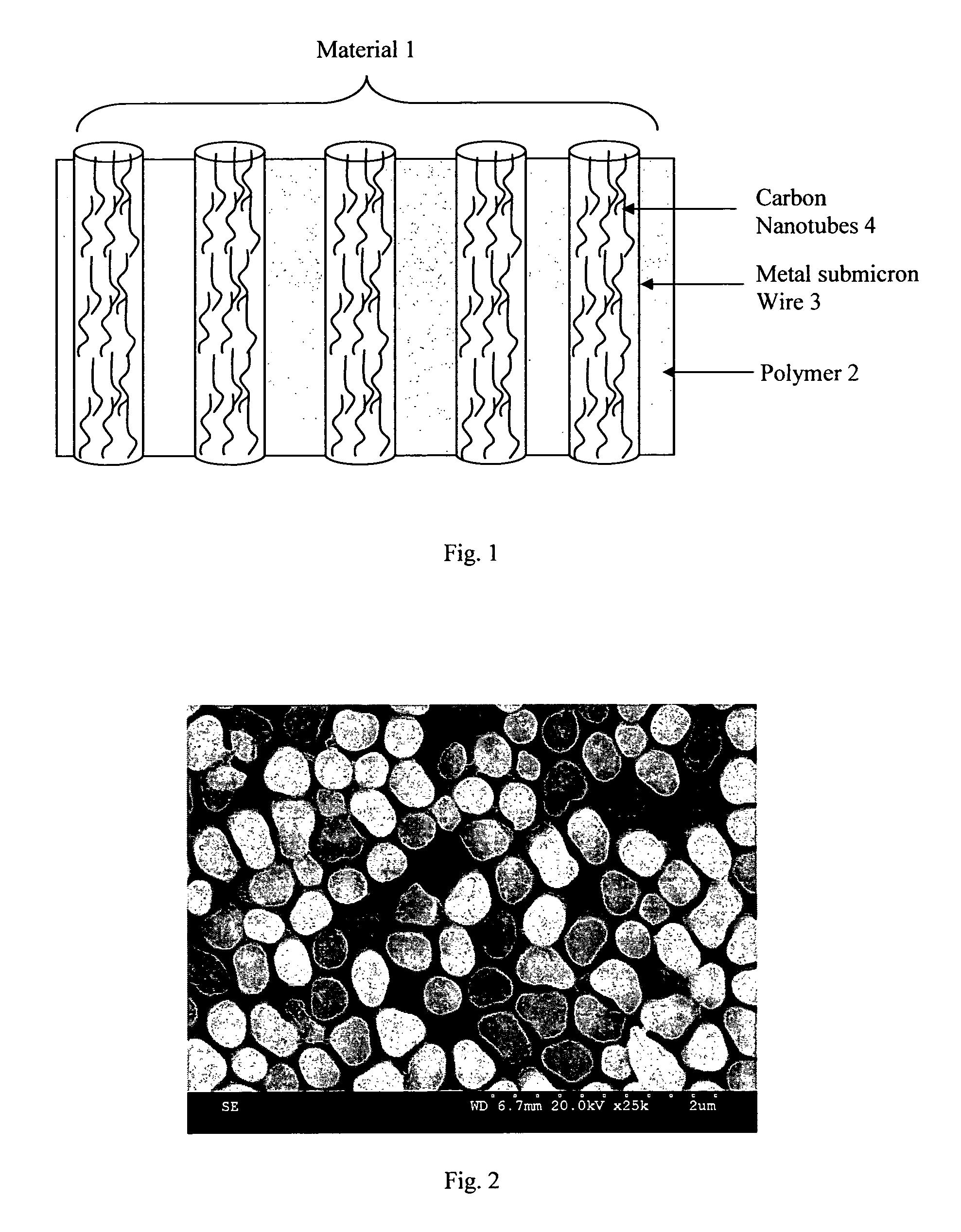
[0032]FIG. 1 is a diagram illustrating a thermal interface material of the invention;

[0033]FIG. 2 is a scanning electron micrograph showing sub-micron wires of the material;

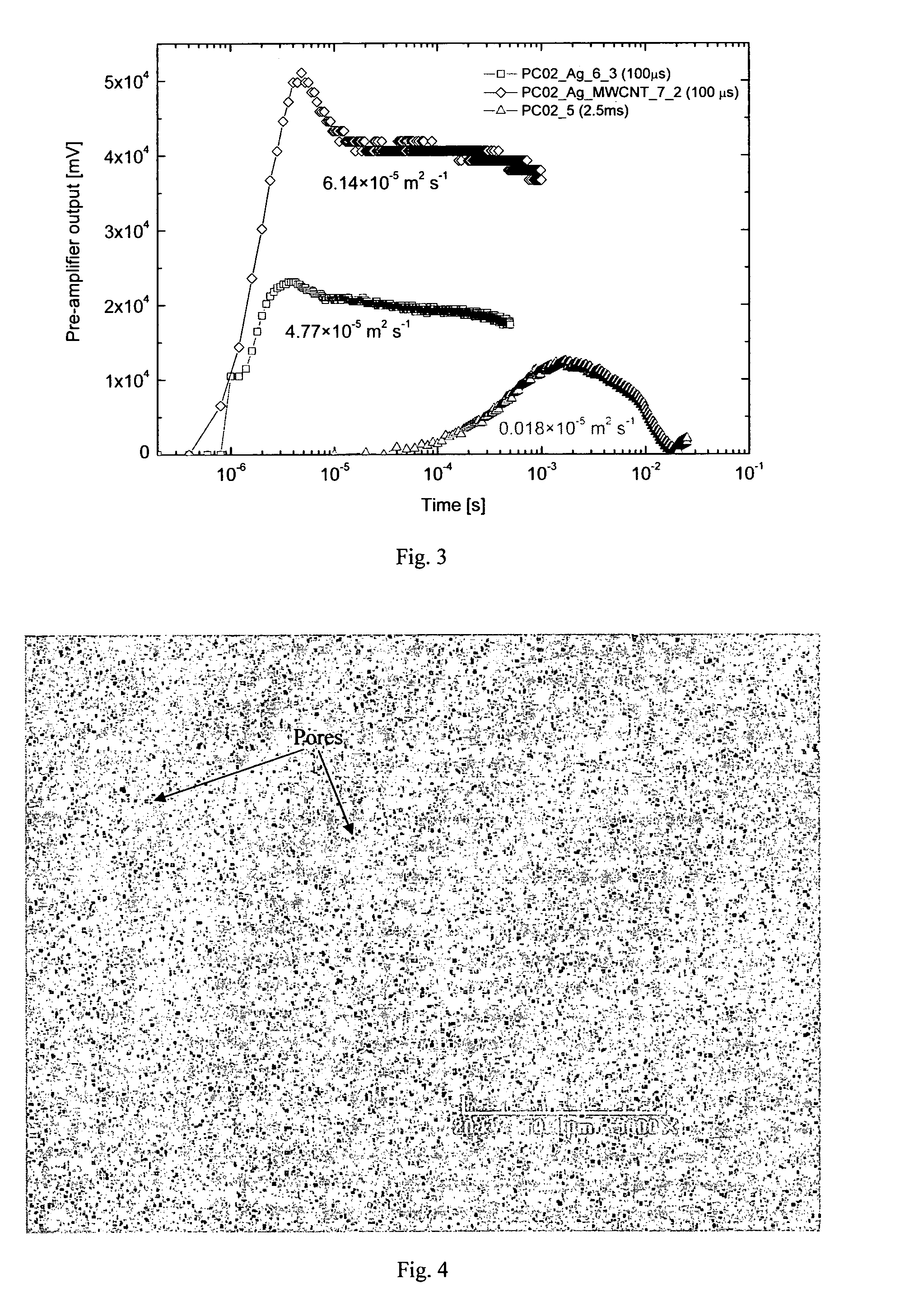
[0034]FIG. 3 is a set of plots illustrating enhancement of thermal diffusivity of a materials of the invention, the value 6.14×10⁻⁵m2s−1 being for the material of the invention, the value 4.77×10⁻⁵m2s−1 being for the polycarbonate template with only silver sub-micron wires, and the value 0.018×10⁻⁵m2s−1 being for the polycarbonate template only;

[0035]FIG. 4 is a scanning electron micrograph showing pores on the top surface of a polycarbonate template before processing;

[0036]FIG. 5 is a schematic of an apparatus for electrodeposition of silver / carbon nanotube composites inside pores of polyc...


PUM

PropertyMeasurementUnit
diameteraaaaaaaaaa
diameteraaaaaaaaaa
lengthaaaaaaaaaa

Abstract

A thermal interface material (1) comprises a bulk polymer (2) within which is embedded sub-micron (c. 200 to 220 nm) composite material wires (3) having Ag and carbon nanotubes (“CNTs”) 4. The CNTs are embedded in the axial direction and have diameters in the range of 9.5 to 10 nm and have a length of about 0.7 μm. In general the pore diameter can be in the range of 40 to 1200 nm. The material (1) has particularly good thermal conductivity because the wires (3) give excellent directionality to the nanotubes (4)—providing very low resistance heat transfer paths. The TIM is best suited for use between semiconductor devices (e.g. power semiconductor chip) and any type of thermal management systems for efficient removal of heat from the device.

Description

RELATED APPLICATIONS[0001]The subject application is a U.S. National Stage application that claims the priority of International Application No. PCT / IE2008 / 000047, filed on 23 Apr. 2008, which claims the priority of Irish National Application Nos.: 2007 / 0298, filed on 23 Apr. 2007, and 2008 / 0135, filed on 22 Feb. 2008, the contents of which are herein incorporated by reference in their entirety.FIELD OF THE INVENTION[0002]The invention relates to a thermal interface material (“TIM”) for uses such as high thermal conductivity.[0003]One of the main limitations in power semiconductor device cooling is the microscopic unevenness and non-planarity between the mating surfaces (chip and heat sink). Asperities on each of the surfaces prevent the two solids forming a thermally perfect contact. Therefore there have been proposals to move away from TIMs in the form of bulk rigid bodies such as Cu films.[0004]Thermal interface materials are therefore used to provide a reliable heat conduction p...

Claims


Application Information

Patent Timeline
Patent Type & Authority Patents(United States)
IPC IPC(8): H01L23/34C25D15/00B32B3/24H01L23/373C25D5/02
CPCC08K7/02H01L23/3733H01L2924/0002C08K9/02H01L23/3736H01L2224/29499Y10T428/24124Y10T428/24174Y10T428/24182Y10T428/24322Y10T428/24331Y10T428/25Y10T428/26Y10T428/268Y10T428/2913Y10T428/2916Y10T428/2918Y10T428/2935Y10T428/294Y10T428/2973Y10T428/298Y10T428/2982H01L2924/00
Inventor RAZEEB, KAFIL M.ROY, SAIBALROHAN, JAMES FRANCISNAGLE, LORRAINE CHRISTINE
Owner UNIV COLLEGE CORK NAT UNIV OF IRELAND CORK
Why Eureka
Try Eureka