Organic electroluminescent device having a light-emitting layer comprising a host material of two or more compounds

an electroluminescent device and organic technology, applied in the direction of discharge tube luminescnet screens, natural mineral layered products, etc., can solve the problems of lowering the luminous efficiency, increasing the driving voltage, and increasing the layer composed of arylamine compounds into the light-emitting layer, so as to secure the driving stability of the device, increase the luminous efficiency, and high efficiency

Inactive Publication Date: 2014-04-22
PIONEER CORP +2
View PDF11 Cites 1 Cited by
  • Summary
  • Abstract
  • Description
  • Claims
  • Application Information

AI Technical Summary

Benefits of technology

[0021]In applications of organic EL devices to display devices such as flat panel displays, it is necessary to enhance the luminous efficiency of the device and, at the same time, to fully secure the driving stability of the device. Under the aforementioned circumstances, an object of this invention is to provide an organic EL device of high efficiency, good driving stability, and practical usefulness. Another object of this invention is to provide a phosphorescent organic EL device emitting red light.
[0022]The inventors of this invention have conducted intensive studies, found as a result that the use of a combination of plural compounds of a specified structure in the light-emitting layer of an organic EL device can solve the aforementioned problems, and completed this invention.

Problems solved by technology

However, an organic EL device comprising CBP as a host material in the light-emitting layer has faced a problem that the barrier to injection of holes from the hole-transporting layer composed of an arylamine compound into the light-emitting layer tends to become higher and the driving voltage becomes higher.
On the other hand, CBP has a property of allowing holes to flow more easily than electrons; hence, excess holes tend to flow out to the side of the electron-transporting layer when CBP is used and this is one cause for lowering of the luminous efficiency.
However, BCP lacks reliability as a hole-blocking material on account of its tendency to crystallize easily even at room temperature and a device containing BCP shows an extremely short lifetime.
On the other hand, BAlq has a Tg of approximately 100° C. and a device containing it is reported to show a relatively long lifetime; however, the hole-blocking ability of BAlq is not sufficient and the luminous efficiency from Ir(ppy)3 becomes lower.
However, BAlq has a property of hindering the flow of holes and, besides, the light-emitting layer must be made relatively thick when a hole-blocking layer is omitted and the problem here is a rise in the driving voltage.
However, the problem with arylamine compounds, typically NPB, has been that the substituents attached to their nitrogen atom tend to move easily due to the molecular structure of these compounds thereby increasing the probability of nonradiative deactivation of triplet excitons and, as a result, the efficiency becomes lower.
However, the documents do not teach their use as a phosphorescent host material.

Method used


Image

  • Organic electroluminescent device having a light-emitting layer comprising a host material of two or more compounds
  • Organic electroluminescent device having a light-emitting layer comprising a host material of two or more compounds
  • Organic electroluminescent device having a light-emitting layer comprising a host material of two or more compounds

Examples


example 1

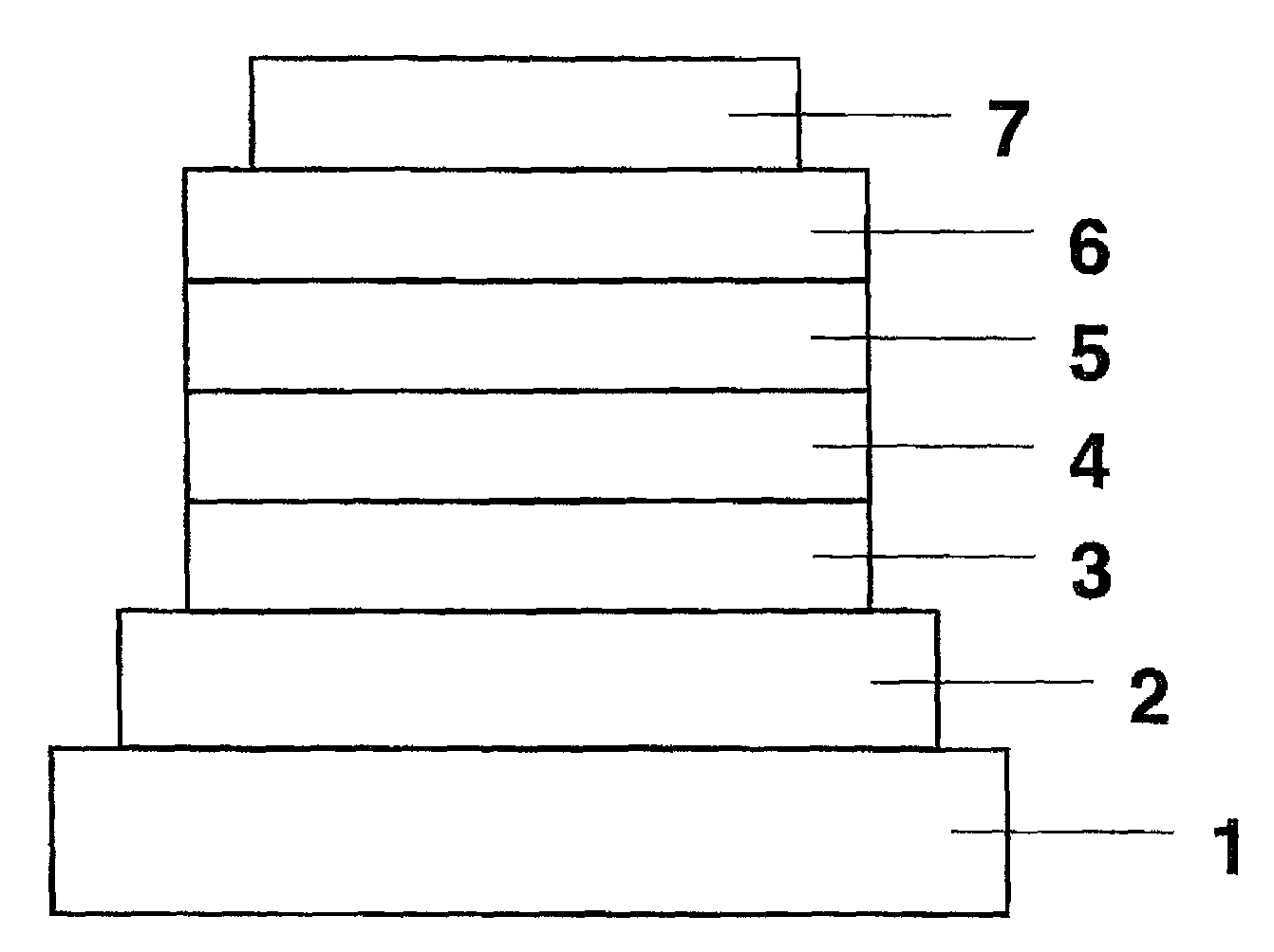
[0081]An organic EL device constituted as in FIG. 1 with addition of an electron-injecting layer was fabricated. Applying the vacuum deposition process at a degree of vacuum of 4.0×10⁻⁴ Pa, the constituent layers were deposited in thin film one upon another on a glass substrate on which a 110 nm-thick ITO anode had been formed. First, CuPC was deposited on the ITO anode to a thickness of 30 nm as a hole-injecting layer and NPB was deposited to a thickness of 50 nm as a hole-transporting layer.

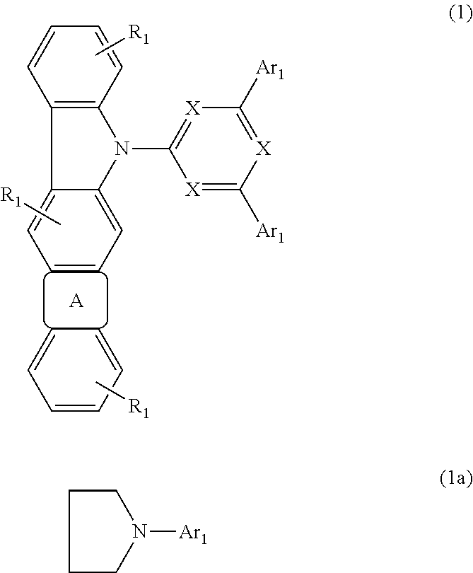
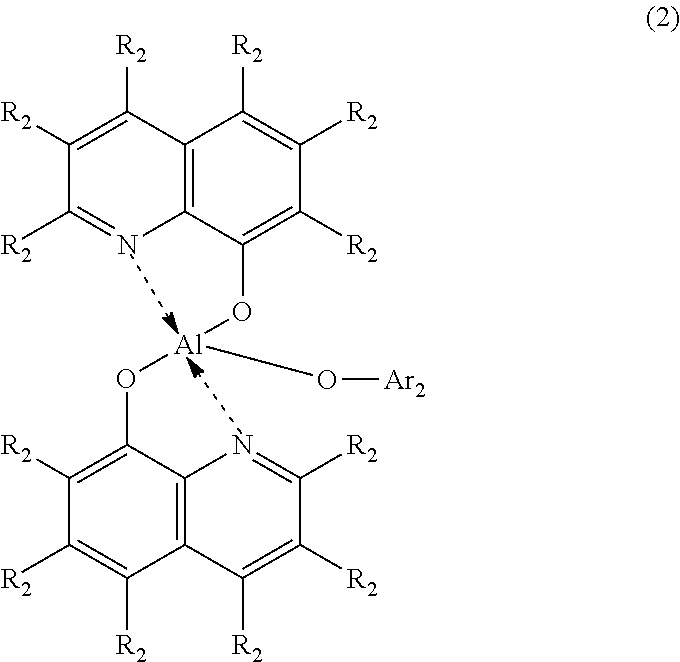
[0082]Then, a light-emitting layer was formed on the hole-transporting layer by co-depositing illustrated Compound 1-1, illustrated Compound 2-1, and illustrated Compound 3-1 as a host material and Ir(piq)2acac (illustrated Compound 4-8) as a dopant from different evaporation sources to a thickness of 40 nm. At this point, the co-deposition was performed under such conditions as to control the concentration of Ir(piq)2acac at 6.0 wt % and the weight ratio illustrated Compound 1-1:illustrated Co...

examples 2-13

[0084]Organic EL devices were fabricated as in Example 1 with the exception of changing the host materials incorporated in the light-emitting layer as shown in Table 1 and their luminous characteristics and luminance half life were evaluated. The vacuum deposition of the compounds of general formulas (1), (2), and (3) was performed under such conditions as to control the weight ratio after the vacuum deposition at 1:1 when two kinds were used or at 1:1:1 when three kinds were used. The results are shown in Table 1. The maximum wavelength of the spectrum of light emitted from the device was 620 nm and this proves that light is emitted from Ir(piq)2acac.

example 14

[0087]An organic EL device constituted as in FIG. 1 with addition of an electron-injecting layer was fabricated. Applying the vacuum deposition process at a degree of vacuum of 4.0×10⁻⁴ Pa, the constituent layers were deposited in thin film one upon another on a glass substrate on which a 110 nm-thick ITO anode had been formed. First, CuPC was deposited on the ITO anode to a thickness of 30 nm as a hole-injecting layer and then NPB was deposited to a thickness of 50 nm as a hole-transporting layer.

[0088]Next, a light-emitting layer was formed on the hole-transporting layer by co-depositing illustrated Compound 2-1 and illustrated Compound 3-1 as a host material and Ir(piq)2acac (illustrated Compound 4-8) as a dopant from different evaporation sources to a thickness of 40 nm. At this point, the co-deposition was performed under such conditions as to control the concentration of Ir(piq)2acac at 6.0 wt % and the weight ratio illustrated Compound 2-1:illustrated Compound 3-1 at 1:1. The...


PUM

PropertyMeasurementUnit
emission peak wavelengthaaaaaaaaaa
Tgaaaaaaaaaa
emission wavelengthaaaaaaaaaa

Abstract

Disclosed is an organic electroluminescent device (organic EL device) that is improved in the luminous efficiency, fully secured of the driving stability, and of a simple structure. The organic EL device comprises a light-emitting layer between an anode and a cathode piled one upon another on a substrate and the said light-emitting layer comprises (A) a phosphorescent dopant whose emission peak wavelength is longer than 600 nm and (B) a host material. The host material contains at least two kinds of compounds selected from two or more kinds of derivatives included in (b1) N-substituted indolocarbazole derivatives, (b2) derivatives of 8-hydroxyquinoline aluminum complex, and (b3) bisindolocarbazole derivatives.

Description

FIELD OF TECHNOLOGY[0001]This invention relates to a novel organic electroluminescent device (hereinafter referred to as organic EL device) and, more particularly, to an organic EL device that uses a phosphorescent dopant emitting red light and a plurality of host compounds of a specified structure in the light-emitting layer.BACKGROUND TECHNOLOGY[0002]An organic EL device in the simplest structure is generally constituted of a light-emitting layer and a pair of counter electrodes sandwiching the said light-emitting layer. The device functions by utilizing the following phenomenon; upon application of an electrical field between the electrodes, electrons are injected from the cathode and holes are injected from the anode and the excited state created by recombination of the electrons and holes in the light-emitting layer returns to the ground state with emission of light.[0003]In recent years, organic thin films have been used in the development of organic EL devices. In particular,...

Claims


Application Information

Patent Timeline
Patent Type & Authority Patents(United States)
IPC IPC(8): H01L51/54C09K11/06
CPCC09K2211/1029C09K11/06C09K2211/186H01L51/0081C07D519/00H01L51/0067H01L51/0072C07D487/04H01L51/0078H01L51/0085H01L51/5016H05B33/14H10K85/654H10K85/6572H10K85/311H10K85/324H10K85/342H10K50/11H10K2101/10Y10S428/917
Inventor YAMAMOTO, TOSHIHIROKAI, TAKAHIROKOMORI, MASAKITSUJI, TAISHITAKAHASHI, YASUHIROYUKI, TOSHINAONAKAJIMA, YUSUKEHOSHI, TOMOAKIASAKA, JIRO
Owner PIONEER CORP
Why Eureka
Try Eureka