External storage device and method of manufacturing external storage device

a technology of external storage and manufacturing method, which is applied in the direction of magnets, magnets, instruments, etc., can solve the problems of difficulty in difficulty in reducing the cost of manufacturing imitation products of semiconductor chips, so as to achieve the effect of sufficiently ensuring the tamper-proof property of an external storage devi

Active Publication Date: 2014-04-22
RENESAS ELECTRONICS CORP
View PDF31 Cites 1 Cited by
  • Summary
  • Abstract
  • Description
  • Claims
  • Application Information

AI Technical Summary

Benefits of technology

[0008]The inventor has made the present invention noting that when the content cannot be used if the content is not read by a dedicated device, the tamper-proof property can be ensured by making it impossible to form an external storage device with general products even if the content is read and copied.
[0010]When the content is stored in the external storage device according to the embodiment of the present invention and is read by a dedicated device, it is necessary to manufacture an external storage device with the same structure as an imitation product of the external storage device according to the embodiment of the present invention in order to use the duplicated content. In the present invention, the information stored in the storage element is communicated to the outside through the inductor. The inductor is small because the inductor is formed in a semiconductor chip. In other words, it is difficult to form an inductor, which has the same diameter as the inductor in the embodiment of the present invention, without using a semiconductor process. In order to realize a semiconductor process, a large investment in facilities is required. Accordingly, it is difficult to manufacture imitation products of the semiconductor chip in terms of costs. For this reason, according to the embodiment of the present invention, even if the content stored in the external storage device can be read, it is not possible for those who copy the content to prepare an external storage device for storing the content. As a result, the tamper-proof property is improved.
[0013]According to the embodiments of the present invention, a tamper-proof property of an external storage device can be sufficiently ensured.

Problems solved by technology

Thus, it has been difficult to sufficiently ensure the tamper-proof property.
Accordingly, it is difficult to manufacture imitation products of the semiconductor chip in terms of costs.

Method used


Image

  • External storage device and method of manufacturing external storage device
  • External storage device and method of manufacturing external storage device
  • External storage device and method of manufacturing external storage device

Examples


first embodiment

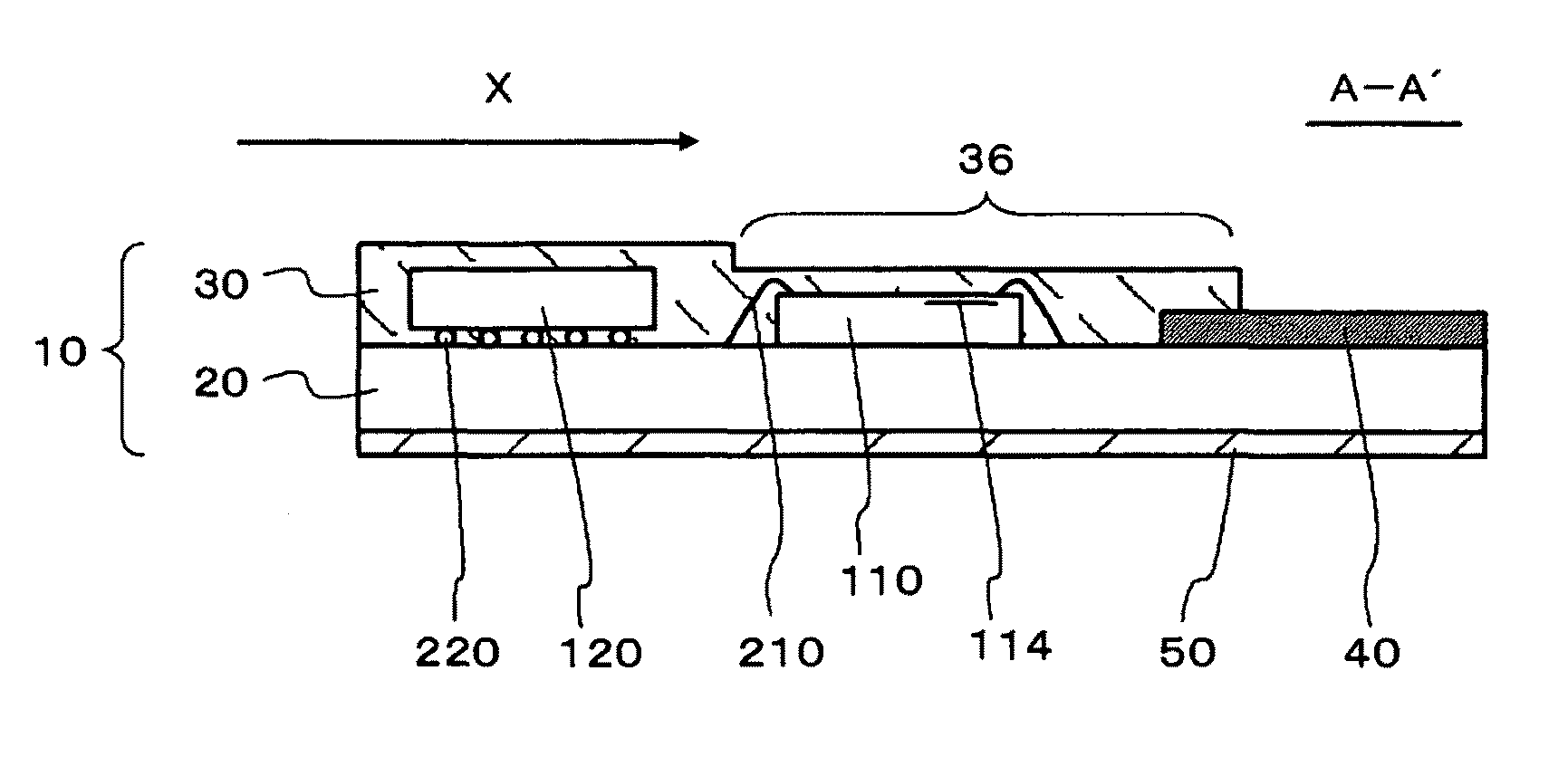
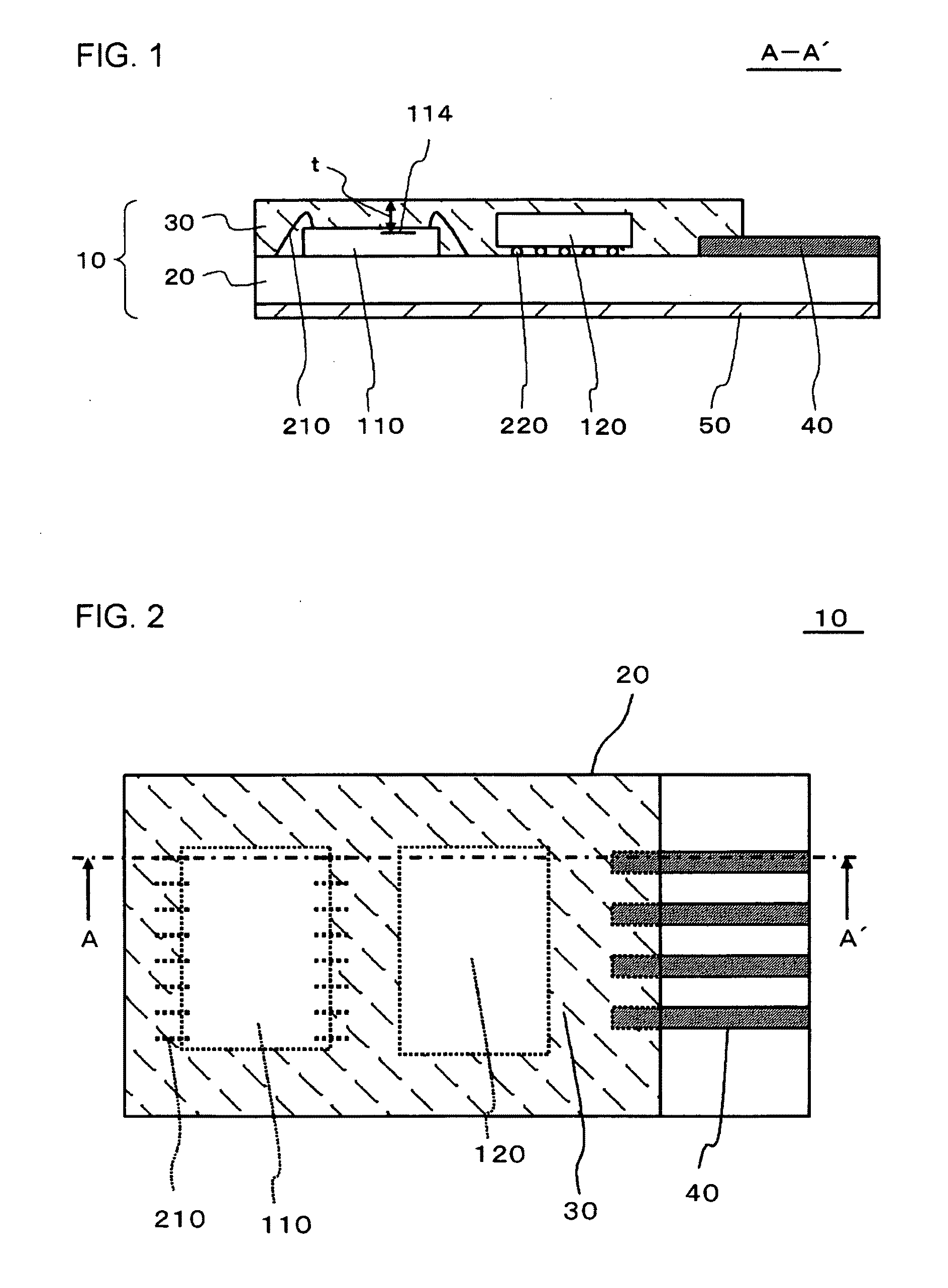
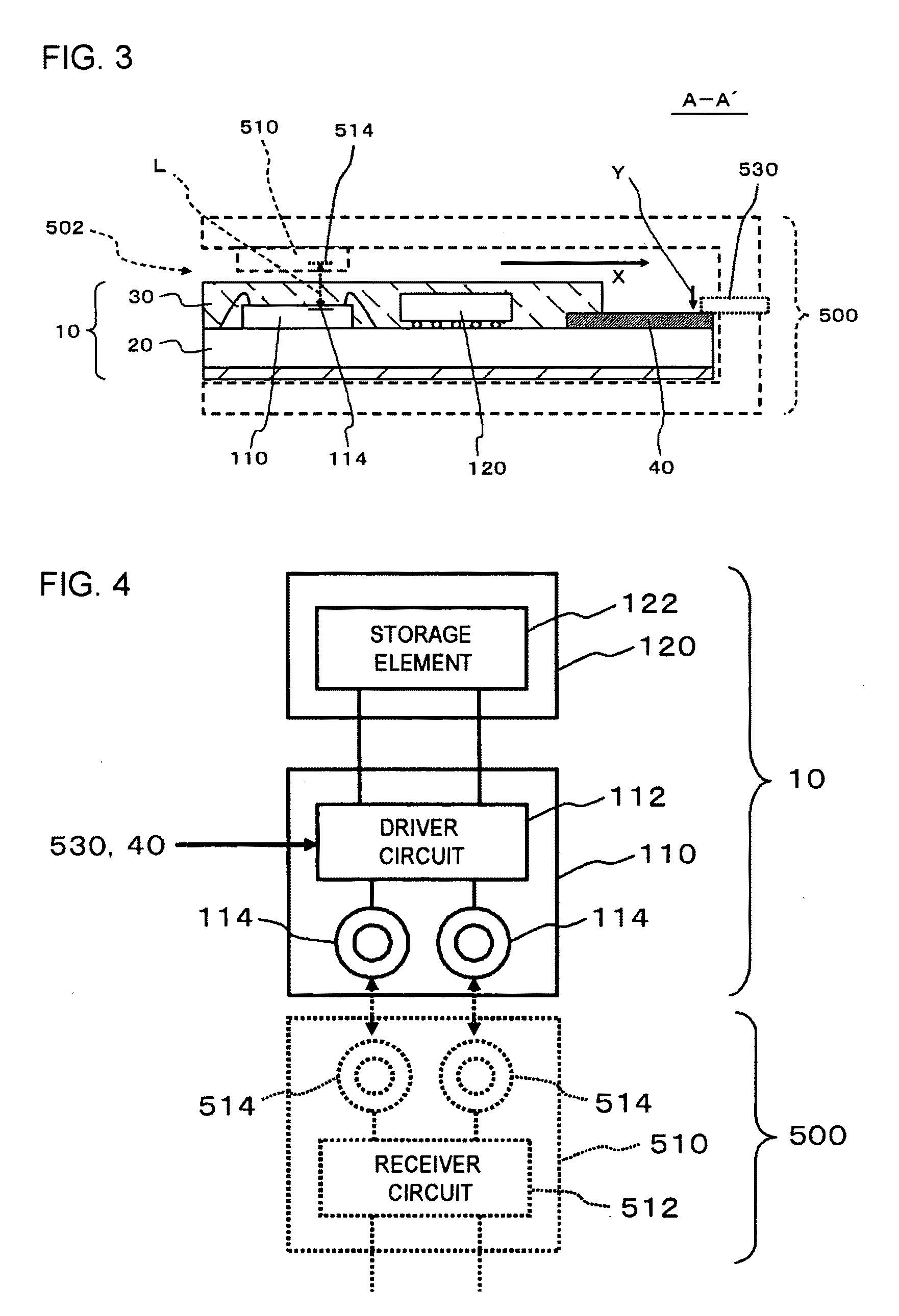
[0046]FIG. 1 is a sectional view showing the configuration of an external storage device 10 according to a The external storage device 10 includes an interconnect substrate 20, at least one semiconductor chip (in an example shown in FIG. 1, two semiconductor chips 110 and 120), a storage element 122 (shown in FIG. 4), an inductor 114, a driver circuit 112 (shown in FIG. 4), an external terminal 40, and a sealing resin layer 30. The semiconductor chips 110 and 120 are disposed on a first surface (for example, an upper surface) of the interconnect substrate 20. The storage element 122 is provided in either of the semiconductor chips 110 and 120. The inductor 114 is also provided in either of the semiconductor chips 110 and 120. The driver circuit 112 is a circuit which drives the inductor 114, and is provided in either of the semiconductor chips 110 and 120. In the present embodiment, the storage element 122 is provided in the semiconductor chip 120, the inductor 114 is provided in t...

third embodiment

[0093]Also in the present embodiment, the same effects as in the third embodiment can be achieved.

[0094]FIG. 15 is a sectional view showing the configuration of an external storage device 10 according to a sixth embodiment and is equivalent to a sectional view taken along the line A-A′ of FIG. 2 in the first embodiment. The external storage device 10 shown in FIG. 15 has the same configuration as the external storage device 10 according to the first embodiment except that a supporting member 140 is provided.

[0095]The supporting member 140 is located between the first surface of the interconnect substrate 20 and the semiconductor chip 110. That is, the supporting member 140 is provided on the first surface of the interconnect substrate 20, and the semiconductor chip 110 is provided on the supporting member 140.

[0096]Also in the present embodiment, the same effects as in the first embodiment can be achieved. In addition, the upper surface of the semiconductor chip 110 may be located b...

ninth embodiment

[0117]First, the sealing resin layer 30 is also formed at the second surface side of the interconnect substrate 20. Here, the sealing resin layer 30 does not cover the external terminal 40. In addition, the penetrating hole 24, the conductive film 26, the through hole 27, and the openings 52 and 62 shown in the ninth embodiment are formed in a portion of the interconnect substrate 20 which does not become either of the external storage devices 10. Accordingly, the external storage device 10 does not have the penetrating hole 24, the conductive film 26, the through hole 27, and the openings 52 and 62.

[0118]FIG. 21 is a plan view showing the shape of the interconnect substrate 20 in the present embodiment. The interconnect substrate 20 has a plurality of through holes 28 and 29 at positions which do not overlap the semiconductor chips 110 and 120 and an interconnect on the interconnect substrate 20. The through hole 28 is located in a region of the interconnect substrate 20 which beco...


PUM

PropertyMeasurementUnit
diameteraaaaaaaaaa
thicknessaaaaaaaaaa
distanceaaaaaaaaaa

Abstract

A storage element is provided in a semiconductor chip, and an inductor and a driver circuit are provided in another semiconductor chip. An external terminal is a contact type terminal, and at least some external terminals are a power supply terminal and a ground terminal. A sealing resin layer is formed over a first surface of an interconnect substrate and seals the semiconductor chips but does not cover the external terminal. The inductor is formed at a surface of the semiconductor chip not facing the interconnect substrate.

Description

[0001]This application is based on Japanese patent application NO. 2009-284348, the content of which is incorporated hereinto by reference.BACKGROUND[0002]1. Technical Field[0003]The present invention relates to an external storage device with a high tamper-proof property and a method of manufacturing an external storage device.[0004]2. Related Art[0005]In the business of making money by selling content, an external storage device in which the content is stored, for example, a memory card may be sold. In such a business model, the content stored in an external storage device is increasingly read by a dedicated device in recent years. When the external storage device is formed by a typical memory card, the information is transmitted to the dedicated device using a contact type external terminal (for example, see Japanese Unexamined patent publication NO. 2009-105126).[0006]In addition, Japanese Unexamined patent publication NO. 2002-083894 discloses performing non-contact type transm...

Claims


Application Information

Patent Timeline
Patent Type & Authority Patents(United States)
IPC IPC(8): H01L23/48H01F7/06H05K7/20
CPCH05K1/117H01L2924/01006H05K2203/1316H05K2201/0949G11C5/005H01L23/49855H01L2224/48227H01L2924/1815H05K3/284H01L23/3121H01L2924/01082H01L2224/49175H01L23/48H01L2224/48225H01L2224/48091H01L23/562H05K2203/0228H05K2201/09845H01L2924/01005H01L2924/01033H01L27/0688H01L2924/01079H01L24/97H01L2224/32225H01L2924/014H01L2224/48228H01L24/48H01L2224/73265H01L21/565H05K3/0052H01L21/561H01L24/49H01L23/5227H01L2924/01029H01L2224/16225H01L2224/97H05K2203/1572H01L2924/12041H01L28/10Y10T29/4902Y10T29/4913H01L2924/181H01L2924/15183H01L2924/00014H01L2224/81H01L2924/00H01L2924/00012H01L2224/45099H01L2224/45015H01L2924/207
Inventor NAKASHIBA, YASUTAKAOGAWA, KENTA
Owner RENESAS ELECTRONICS CORP
Why Eureka
Try Eureka