Lighting device and method for manufacturing the same
a technology of light-emitting devices and manufacturing methods, which is applied in the manufacture of electrode systems, electric discharge tubes/lamps, instruments, etc., can solve the problems of not reaching 100% efficiency in extracting light from the inside of light-emitting elements to the air, and achieve the effect of reducing manufacturing costs and high efficiency
- Summary
- Abstract
- Description
- Claims
- Application Information
AI Technical Summary
Benefits of technology
Problems solved by technology
Method used
Image
Examples
embodiment 1
Structure of Lighting Device
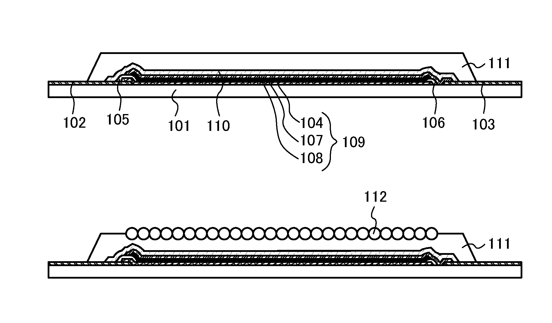
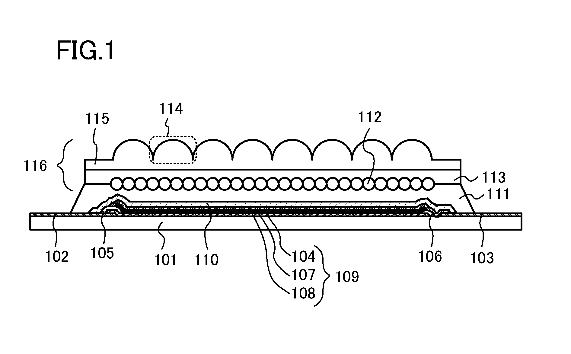
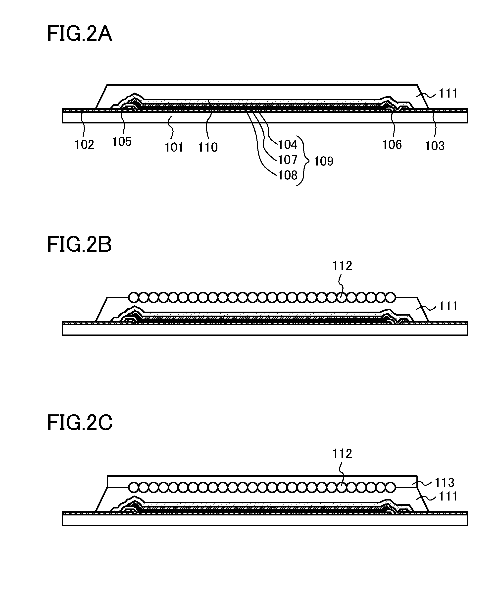
[0060]FIG. 1 shows a cross-sectional view of a lighting device of this embodiment. The lighting device shown in FIG. 1 includes a substrate 101, a first terminal 102, a second terminal 103, a first electrode 104 electrically connected to the first terminal 102, and a partition wall 105 and a partition wall 106 which are formed to cover edge portions of the first electrode 104. Further, the lighting device shown in FIG. 1 includes an EL layer 107 provided over the first electrode 104, the partition wall 105, and the partition wall 106, and a second electrode 108 provided over the EL layer 107 and the partition wall 106 and electrically connected to the second terminal 103. The first electrode 104, the EL layer 107, and the second electrode 108 form a light-emitting element layer 109.
[0061]Note that in the lighting device shown in FIG. 1, one light-emitting element layer 109 is provided as an example; however, the present invention is not limited to this. I...
embodiment 2
Structure of Lighting Device
[0141]FIG. 5 shows a cross-sectional view of a lighting device of this embodiment. The lighting device shown in FIG. 5 includes the substrate 101, the first terminal 102, the second terminal 103, the first electrode 104 electrically connected to the first terminal 102, and the partition wall 105 and the partition wall 106 which are formed to cover edge portions of the first electrode 104. Further, the lighting device shown in FIG. 5 includes the EL layer 107 provided over the first electrode 104, the partition wall 105, and the partition wall 106, and the second electrode 108 provided over the EL layer 107 and the partition wall 106 and electrically connected to the second terminal 103. The first electrode 104, the EL layer 107, and the second electrode 108 form the light-emitting element layer 109.
[0142]Note that in the lighting device shown in FIG. 5, one light-emitting element layer 109 is provided as an example; however, the present invention is not l...
embodiment 3
[0198]In this embodiment, structures of microlens arrays, methods for manufacturing the microlens array, and lighting devices, which are different from those in Embodiment 1 and Embodiment 2, will be described.
[0199]First, steps up to the manufacturing step shown in FIG. 2B, i.e., the steps of scattering the granules 112 over the resin layer 111 in an uncured state and curing the resin layer 111 are performed according to the description in Embodiment 1 (see FIG. 8A).
[0200]Next, a resin that is the material of the resin layer 113 in an uncured state is applied over the resin layer 111 in which the granule 112 is embedded (see FIG. 8B).
[0201]A plurality of granules 117 each having the diameter greater than that of the granule 112 is arranged over the uncured resin layer 113. Next, the resin layer113 is cured (see FIG. 8C).
[0202]Through the above, the plurality of granules 112 is provided at the interface between the resin layer 111 and the resin layer 113. In addition, the plurality ...
PUM
 Abstract
Description
Claims
Application Information
 - R&D
- Intellectual Property
- Life Sciences
- Materials
- Tech Scout
- Unparalleled Data Quality
- Higher Quality Content
- 60% Fewer Hallucinations
Browse by: Latest US Patents, China's latest patents, Technical Efficacy Thesaurus, Application Domain, Technology Topic, Popular Technical Reports.
© 2025 PatSnap. All rights reserved.Legal|Privacy policy|Modern Slavery Act Transparency Statement|Sitemap|About US| Contact US: help@patsnap.com


