
Shift register and electronic device using the same

a technology of shift register and electronic device, which is applied in the direction of digital storage, semiconductor devices, instruments, etc., can solve the problems of increasing the manufacturing cost of shift register and display device using the driver circuit, and many registers in the shift register connected in parallel end up in waste, so as to improve the reliability of electronic device, suppress manufacturing cost, and increase manufacturing yield

Inactive Publication Date: 2005-12-15
SEMICON ENERGY LAB CO LTD
View PDF27 Cites 26 Cited by
  • Summary
  • Abstract
  • Description
  • Claims
  • Application Information

AI Technical Summary

Benefits of technology

[0007] A plurality of shift registers connected in parallel, however, could lead to increase the manufacturing cost of a driver circuit and a display device using the driver circuit. In particular, it is quite unlikely that a plurality of registers are broken in one shift register, therefore, many of the registers in the shift registers connected in parallel end up in waste. Accordingly, it is one of the features of the invention to provide a shift register which can function normally even when part of the registers is broken while suppressing the increase in manufacturing cost as little as possible, and to provide an electronic device using the shift register.
[0008] It is another feature of the invention to provide a shift register which can operate normally by a simple operation without being affected by a broken register, and to provide an electronic device using the shift register.
[0018] The shift register according to the invention includes r (r is a natural number of one or more) redundant registers connected in series to regular registers, and a switch circuit which selectively connects these regular registers and redundant registers to output lines. Therefore, even when some of the regular registers are broken, a normal operation can be obtained by using the same number of redundant registers as the broken regular registers when the number of the broken regular registers is r or less. Moreover, as it is quite unlikely that all the regular registers are broken, the redundant registers are not required to be provided as many as the regular registers, which can minimize the increase in manufacturing cost. The switch circuit connects normal registers of the upper and lower stages of the broken register by skipping and disabling the broken register, therefore, the broken register does not adversely affect an operation of the normal register.
[0020] The switch circuit including a disable circuit which determines a state of each register from a state of the first switch and disables the register determined to be broken can disable the broken register favorably. Normally, an output of each register is connected to a buffer. The disable circuit stops an operation voltage supply to a buffer corresponding to the broken register, thereby an output of the broken transistor becomes electrically floating to prevent an adverse effect to the normal registers.
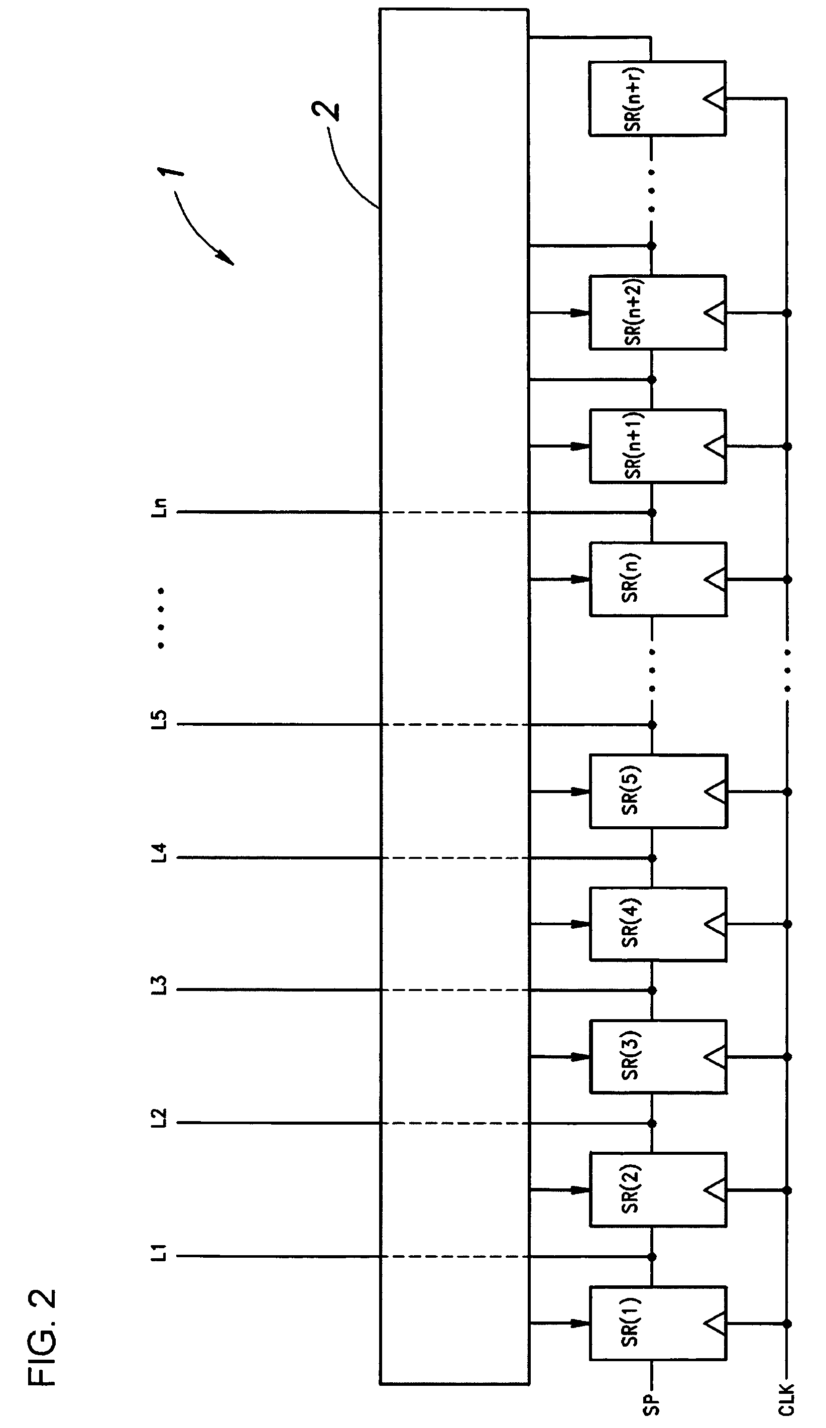
[0024] In the aforementioned shift register which can operate normally with up to two broken registers, provided that the switch circuit includes first and second control signal lines formed of conducting wires each of which has one end connected to the low voltage source (VGND) and the other end connected to the high voltage source (VCC), each control terminal of the first switch is sequentially connected to the first control signal line, a voltage from one of the high voltage source and the low voltage source is supplied as a control signal to each control terminal of the first switch in a normal state, each control terminal of the second switch is sequentially connected to the second control signal line, and a voltage from one of the high voltage source and the low voltage source is supplied to each control terminal of the second switch in a normal state, the states of the first and / or second switches can be changed appropriately by a simple operation to cut off an appropriate part of the first control signal line and / or the second control signal line, thereby the broken register can be skipped and normal registers (regular registers and redundant registers) can be appropriately connected to output lines.
[0025] An electronic device formed by using the aforementioned shift register can increase the manufacturing yield as well as improving the reliability of the electronic device while suppressing the manufacturing cost as little as possible. When the electronic device includes a display device, in particular, an electronic device having high reliability which can operate normally even with some broken registers in the shift registers by using the aforementioned shift register in a driver circuit (a scan line driver circuit and / or a signal line driver circuit) of the display device.

Problems solved by technology

A plurality of shift registers connected in parallel, however, could lead to increase the manufacturing cost of a driver circuit and a display device using the driver circuit.
In particular, it is quite unlikely that a plurality of registers are broken in one shift register, therefore, many of the registers in the shift registers connected in parallel end up in waste.

Method used


Image

  • Shift register and electronic device using the same
  • Shift register and electronic device using the same
  • Shift register and electronic device using the same

Examples


Embodiment Construction

[0041] Hereinafter described with reference to drawings is an embodiment mode of the invention.

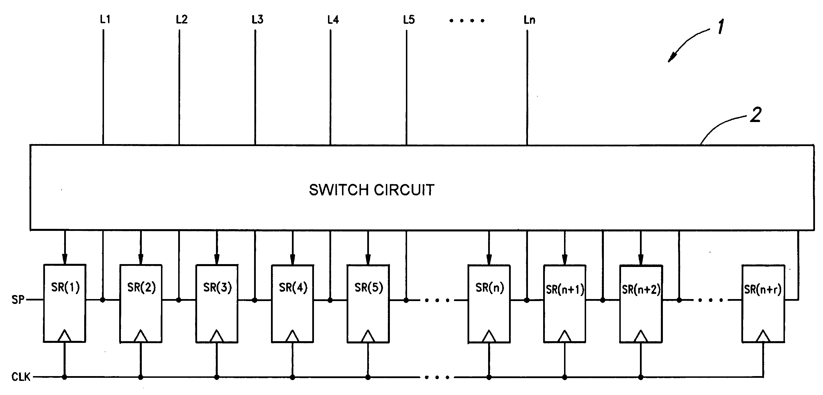
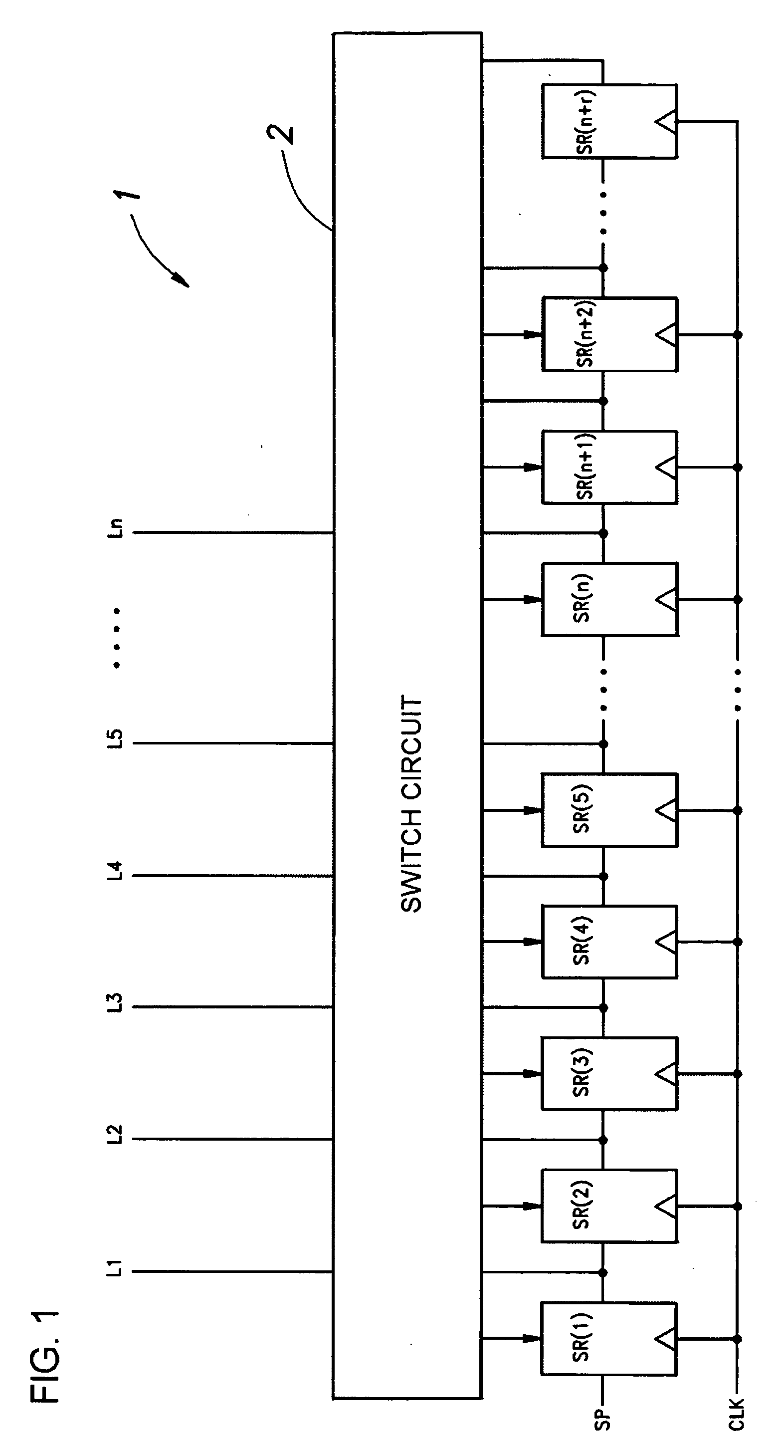
[0042]FIG. 1 is a block diagram showing a preferred embodiment mode of the shift register according to the invention. A shift register 1 includes n regular registers SR(1) to SR(n) connected in series and n output lines L1 to Ln corresponding to the n regular registers SR(1) to SR(n). Further, the shift register 1 includes r redundant registers SR(n+1) to SR(n+r) connected in series to the lower stage of the regular registers SR(1) to SR(n) and a switch circuit 2 provided between the regular and redundant registers SR(1) to SR(n+r) and the output lines L1 to Ln. A clock signal CLK is inputted to the registers SR(1) to SR(n+r). A start pulse SP inputted to the register SR(1) of the input terminal is sent to the register of lower stages in synchronization with the clock signal.

[0043] In the case where none of the regular registers SR(1) to SR(n) are broken, the switch circuit 2 connects ou...


PUM

PropertyMeasurementUnit
operation voltageaaaaaaaaaa
voltageaaaaaaaaaa
luminanceaaaaaaaaaa

Abstract

The invention provides a shift register which can function normally even with an abnormal register or a broken register while suppressing the manufacturing cost as little as possible. The shift register of the invention includes n regular registers (SR(1) to SR(n)) connected in series and n output lines (L1 to Ln) corresponding to the n regular registers, r (r≦n) redundant registers (SR(n+1) to SR(n+r)) connected in series to the n regular registers, and a switch circuit for selectively connecting the regular and redundant resistors to output lines. The switch circuit connects the n regular registers to the corresponding output lines in a normal state, connects normal registers of upper and lower stages of the broken register by skipping and disabling the broken register if any, and connects normal regular registers and the same number of redundant registers as the broken registers to the n output lines.

Description

BACKGROUND OF THE INVENTION [0001] 1. Field of the Invention [0002] The present invention relates to a shift register and an electronic device using the same. [0003] 2. Description of the Related Art [0004] In an active matrix display device such as a liquid crystal display device (LCD) and an EL panel, a shift register is used as a driver circuit (scan line driver circuit and signal line driver circuit) for reducing the number of signal input terminals. A shift register is configured by a plurality of registers connected in series. A signal inputted in each register is transferred to a next register according to a clock signal. [0005] In such a driver circuit, a transistor which forms a register in a shift register may be abnormal (or broken) by static electricity and the like. In such a case, a signal is not transferred to a register of lower stage than the abnormal register (or broken register), which causes a defect in display. Such a display device cannot be shipped as a produc...

Claims


Application Information

Patent Timeline
Patent Type & Authority Applications(United States)
IPC IPC(8): G09G3/36G02F1/133G11C19/00G11C29/00H01L21/82H01L21/822H01L27/04
CPCG09G3/3648G09G3/3677G09G3/3688G11C29/86G11C19/00G11C29/848G09G2330/08
Inventor MUTAGUCHI, KOHEI
Owner SEMICON ENERGY LAB CO LTD
Learn More