X-Y address type solid-state image pickup device with an image averaging circuit disposed in the noise cancel circuit

a solid-state image and noise cancelling technology, applied in the direction of color television details, television systems, radio control devices, etc., can solve the problems of large chip area, large capacity of the storage device for storing image data, and complicated logical processing, etc., to suppress manufacturing costs

Inactive Publication Date: 2007-07-10
SOCIONEXT INC
View PDF12 Cites 23 Cited by
  • Summary
  • Abstract
  • Description
  • Claims
  • Application Information

AI Technical Summary

Benefits of technology

[0008]An object of the present invention is to provide an X-Y address type solid-state image pickup device in which a chip area is not increased, manufacturing costs are suppressed, and an image averaging processing can be carried out.

Problems solved by technology

However, in the above conventional image averaging processing, there arise a problem as follows: FIG. 11 schematically shows a pixel array of a light receiving surface of the CMOS image sensor.
. . , and at an even line, similarly, pixels are successively arranged like G, B, G, B, . . . . Accordingly, if an attempt is made to obtain one pixel for each of R, G and B by averaging image signals of R, G and B from 4×4=16 pixels surrounded by a broken line in the drawing, in the foregoing image averaging processing, the logical processing becomes extremely complicated, and further, the capacity of the storage device for storing the image data becomes large.
Thus, if an attempt is made to incorporate an image averaging circuit in the same chip as the CMOS image sensor, there arises a problem that a chip area is largely increased, and manufacturing costs become high.

Method used


Image

  • X-Y address type solid-state image pickup device with an image averaging circuit disposed in the noise cancel circuit
  • X-Y address type solid-state image pickup device with an image averaging circuit disposed in the noise cancel circuit
  • X-Y address type solid-state image pickup device with an image averaging circuit disposed in the noise cancel circuit

Examples


first embodiment

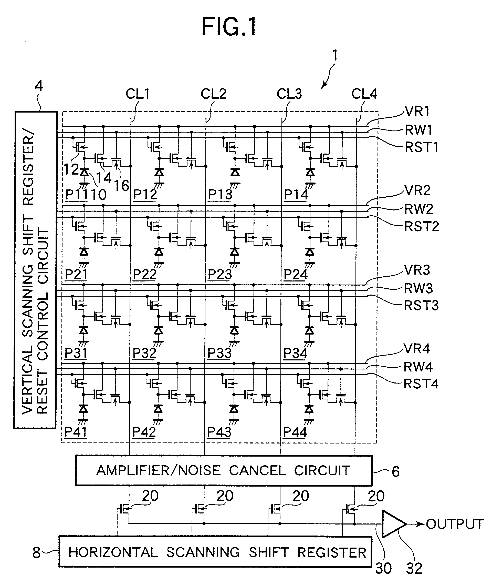
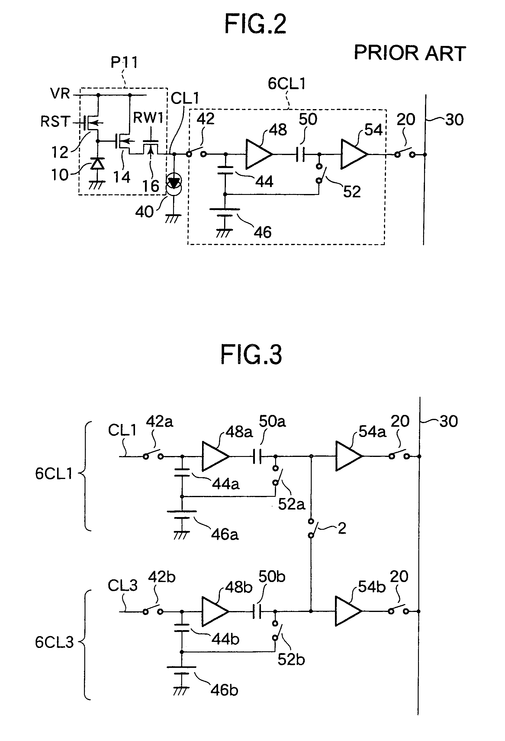
[0021]An X-Y address type solid-state image pickup device according to a first embodiment of the present invention will be described with reference to FIGS. 1 to 3. First, a rough structure of a CMOS image sensor as the X-Y address type solid-state image pickup device according to this embodiment will be described with reference to FIG. 1. FIG. 1 shows a circuit example of 4×4 pixels of a CMOS image sensor 1 including a pixel array of m rows and n columns. Pixel regions P11 to P44 defined by a plurality of vertical selection lines CL1 to CL4 and a plurality of horizontal selection lines RW1 to RW4 are arranged in a matrix form. A photodiode 10 as a photoelectric transducer is formed in each of the pixel regions P11 to P44. As the photoelectric transducer, for example, a photo gate may be used instead of the photodiode 10.

[0022]The CMOS image sensor 1 has, in each of the pixel regions P11 to P44, an APS(Active Pixcel Sensor) structure in which a source follower amplifier 14 constitut...

second embodiment

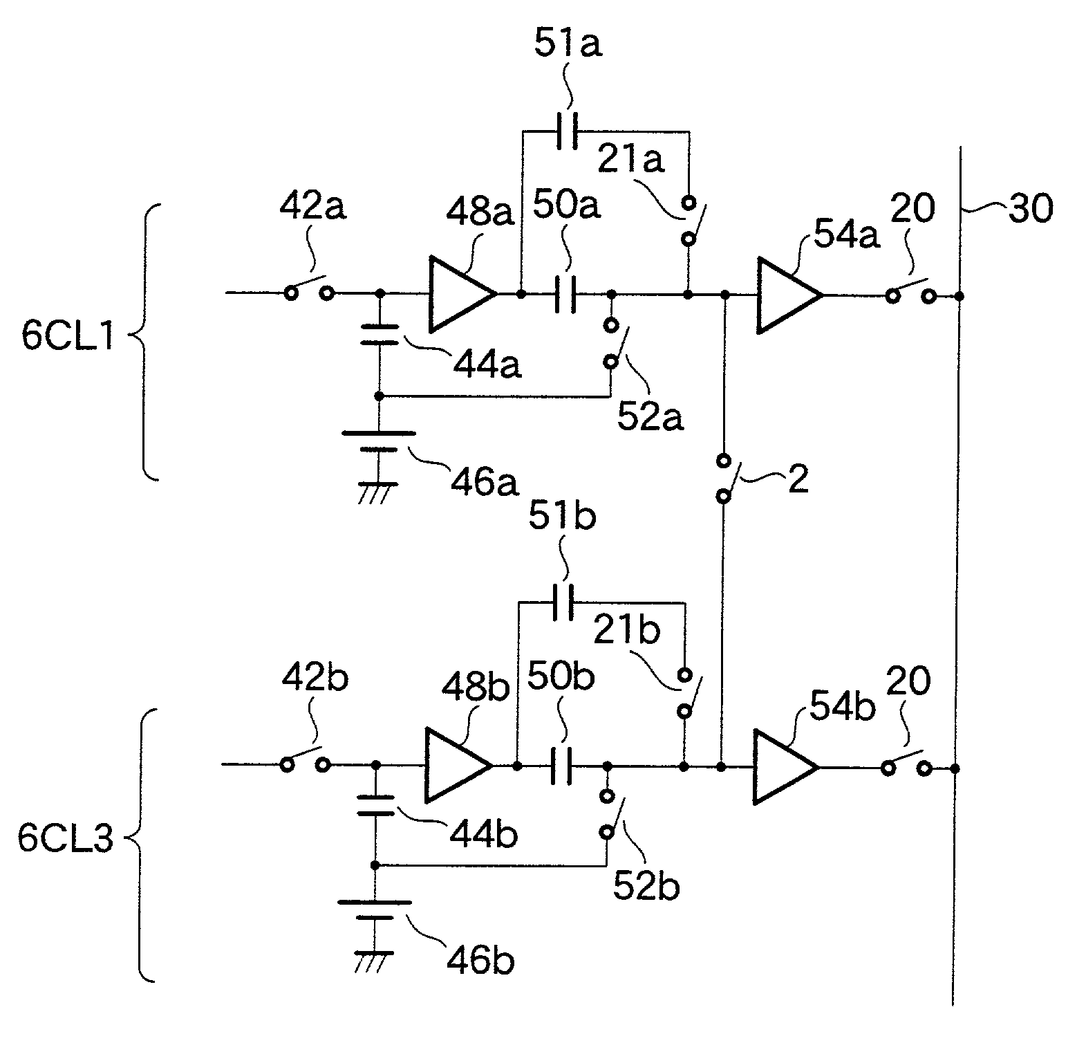
[0046]Next, an X-Y address type solid-state image pickup device according to a second embodiment of the present invention will be described with reference to FIG. 4. The X-Y address type solid-state image pickup device according to this embodiment has a similar structure to the CMOS image sensor of the first embodiment except for a structure of an image averaging circuit. Structural elements having the same operation and function as those of the first embodiment are designated by the same symbols and their description is omitted.

[0047]FIG. 4 shows the image averaging circuit according to this embodiment. A CDS circuit 6CLn according to this embodiment is provided with a circuit for averaging analog image data of at least two pixels arranged in the direction of the extension of a vertical selection line CLn. First, a description will be given of, as an example, a case where for example, pixel regions arranged in the direction of the extension of the vertical selection line CL1 and co...

third embodiment

[0054]Next, an X-Y address type solid-state image pickup device according to a third embodiment of the present invention will be described with reference to FIG. 5. The X-Y address type solid-state image pickup device according to this embodiment has a similar structure to the CMOS image sensor 1 of the second embodiment except for a structure of an image averaging circuit. Structural elements having the same operation and function as the second embodiment are designated by the same symbols and their description is omitted.

[0055]FIG. 5 shows an image averaging circuit according to this embodiment. A CDS circuit 6CL1 shown in FIG. 5 is characterized in that an averaging processing switch 22 is added to a connection point between a CDS capacitance 50 and an amplifier 54 in the structure of the second embodiment shown in FIG. 4.

[0056]An image averaging processing operation in the CDS circuit 6CL1 according to this embodiment will be described. First, only the averaging processing switc...


PUM


Abstract

The invention relates to an X-Y address type solid-state image pickup device manufactured by a CMOS process, and has an object to provide an X-Y address type solid-state image pickup device in which a chip area is not increased, manufacturing costs are suppressed, and an image averaging processing can be carried out. Pixel regions Pmn are arranged in a matrix form in regions defined by horizontal selection lines RWm and vertical selection lines CLn. Each of the pixel regions Pmn includes a photodiode 10, a source follower amplifier 14 for converting an electric charge of the photodiode 10 into a voltage and amplifying it to output image data, and a horizontal selection transistor 16 for outputting the image data to a predetermined one of the vertical selection lines CLn. An amplifier / noise cancel circuit 6 has a built-in image averaging circuit for carrying out an averaging processing of the image data outputted from at least two of the plurality of the pixel regions Pmn.

Description

BACKGROUND OF THE INVENTION[0001]1. Field of the Invention[0002]The present invention relates to a solid-state image pickup device constituted by semiconductor elements, and particularly to an X-Y address type solid-state image pickup device manufactured by a CMOS process.[0003]2. Description of the Related Art[0004]A solid-state image pickup device is roughly classified into a CCD (Charge Coupled Device) solid-state image pickup device constituted by a charge transfer type image sensor, and an X-Y address type solid-state image pickup device in which an image sensor is constituted by, for example, CMOS (Complementary Metal Oxide Semiconductor) transistors. The X-Y address type solid-state image pickup device using a CMOS image sensor (hereinafter suitably abbreviated to a CMOS image sensor) can be manufactured by the same technique as a manufacturing process of a MOSFET, and it is driven by a single power source and has low electric power consumption, and further, various signal pr...

Claims


Application Information

Patent Timeline
Patent Type & Authority Patents(United States)
IPC IPC(8): H04N5/217H01L27/146H04N5/335H04N5/357H04N5/363H04N5/374H04N5/378
CPCH04N5/343H04N5/378H04N5/347H04N25/42H04N25/46H04N25/75H04N25/60
Inventor KOKUBUN, MASATOSHIYAMAMOTO, KATSUYOSIUDO, SHINYAFUNAKOSHI, JUNTSUCHIYA, CHIKARA
Owner SOCIONEXT INC
Why Eureka
Try Eureka