Optical module

a technology of optical modules and optical coupling, applied in the field of optical modules, can solve problems such as the deterioration of optical coupling efficiency, and achieve the effect of improving optical coupling efficiency and substantially eliminating the loss of optical signal propagation

Active Publication Date: 2014-07-01
PANASONIC CORP
View PDF33 Cites 2 Cited by
  • Summary
  • Abstract
  • Description
  • Claims
  • Application Information

AI Technical Summary

Benefits of technology

[0005]This invention has been made in order to solve the aforementioned problem. An object of the invention is to provide an optical module capable of improving the optical coupling efficiency when it is configured to receive an optical signal from an optical fiber with a light receiving element as well as when it is configured to receive an optical signal with an optical fiber.
[0017]Since the internal waveguide is interposed between the mirror portion and the front end of the fiber core of the optical fiber, neither a light flux emitted by the light emitting element nor a light flux emitted from the fiber core of the optical fiber is expanded. Accordingly, propagation loss of the optical signal is substantially eliminated between the mirror portion and the front end of the fiber core of the optical fiber, whereby the optical coupling efficiency can be improved.

Problems solved by technology

This cause a light flux emitted from the core 33a to be expanded, resulting in deterioration of optical coupling efficiency.

Method used


Image

  • Optical module
  • Optical module
  • Optical module

Examples


Embodiment Construction

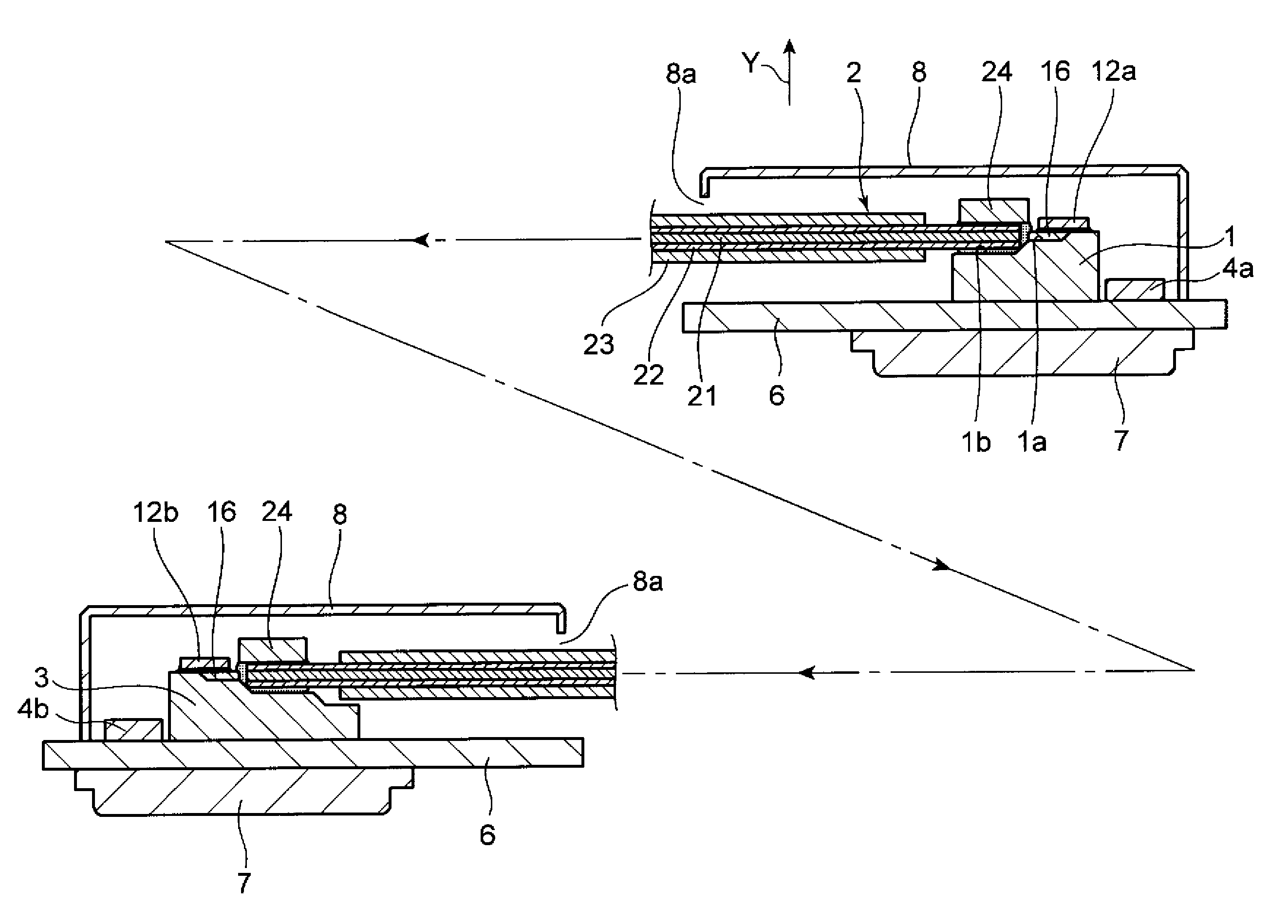
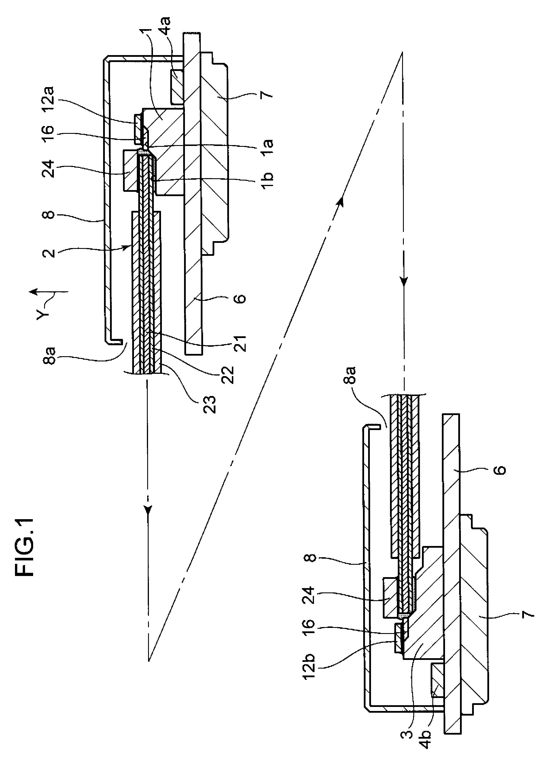
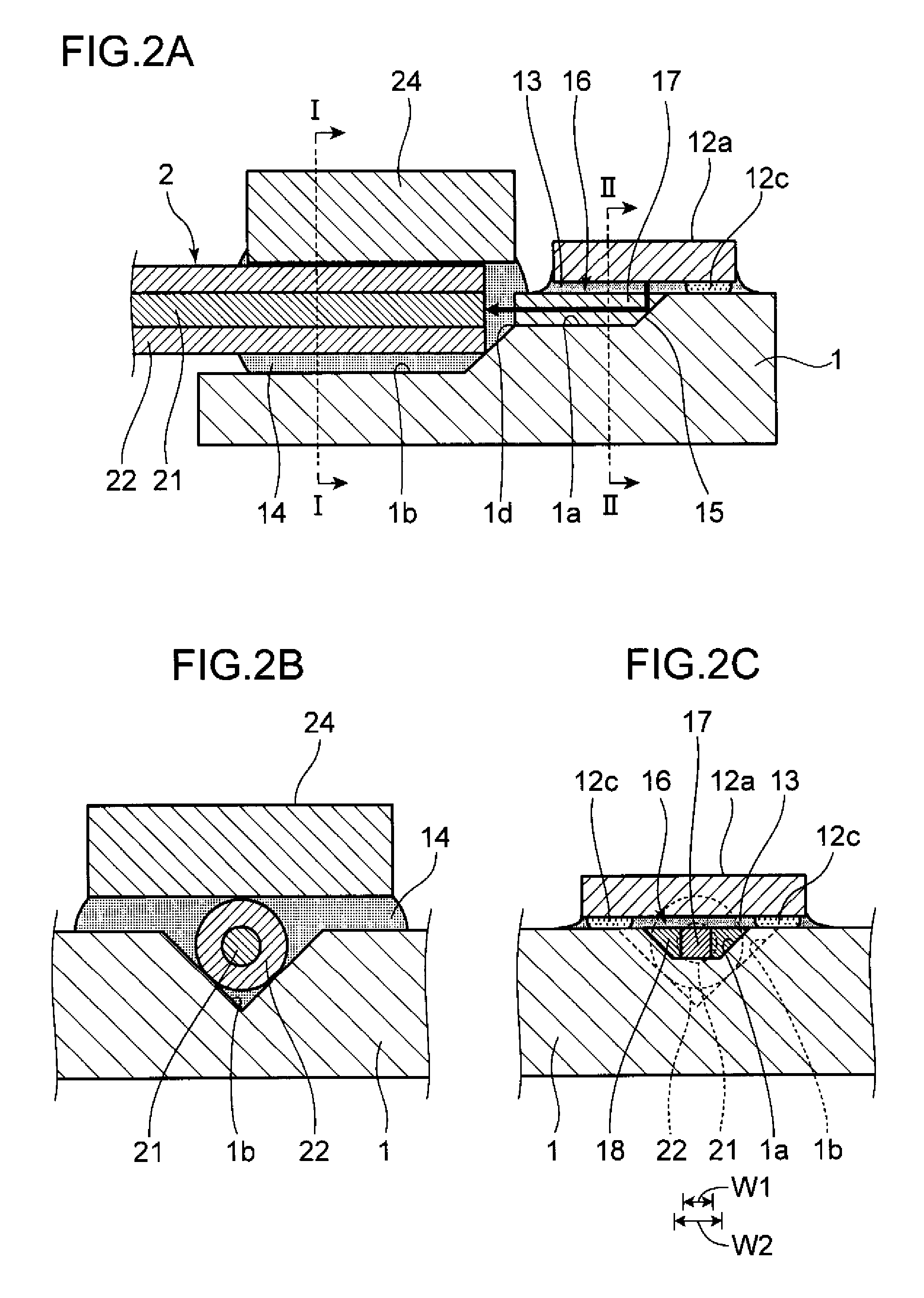
[0036]Preferred embodiments of this invention will be described in detail with reference to the drawings. FIG. 1 is a schematic side view of an optical module according to this invention. FIGS. 2A to 2C are diagrams illustrating a first substrate 1 of the light-emitting optical module of FIG. 1. FIG. 2A is a side cross-sectional view, FIG. 2B is a cross-sectional view taken along the line I-I in FIG. 2A, and FIG. 2C is a cross-sectional view taken along the line II-II in FIG. 2A. FIGS. 3A and 3B are diagrams illustrating the first substrate 1. FIG. 3A is a perspective view, and FIG. 3B is a perspective view of the first substrate 1 having an internal waveguide formed therein. FIGS. 4A and 4B are diagrams illustrating the first substrate 1. FIG. 4A is a perspective view of the first substrate 1 having a light emitting element 12a mounted thereon, and FIG. 4B is a perspective view of the first substrate 1 having an optical fiber 2 inserted therein. FIG. 5 is a perspective view showing...


PUM


Abstract

Disclosed is an optical module which improves optical coupling efficiency either when configured to receive an optical signal from an optical fiber with a light receiving element or when configured to receive an optical signal from a light emitting element with an optical fiber. The optical module includes: a substrate (1) having in the surface thereof a first groove (1a) and a second groove (1b) formed, with this second groove (1b) being configured to have a substantially V-shaped cross section formed deeper than the first groove and being formed in continuation from the first groove; and an internal waveguide (16) provided within the first groove (1a) of the substrate (1). The optical further modules a mirror portion (15) for changing an optical path, provided at the front end of the first groove (1a); an optical element (12a) mounted on the surface of the substrate (1) so as to face the mirror portion (15), and configured to emit an optical signal to a core (17) of the internal waveguide (16) via the mirror portion (15). Moreover, the optical module further includes an optical fiber (2) having a fiber cladding (22) placed within the second groove (1b) and a fiber core (21) optically connected to the core (17) of the internal waveguide (16).

Description

TECHNICAL FIELD[0001]This invention relates to an optical module for transmitting or receiving an optical signal.BACKGROUND ART[0002]Conventionally known optical modules include an optical module described in Patent Document 1. In this optical module, as shown in FIG. 18, a substrate 30 is provided with two V-grooves 31 and 32 having different shapes. A cladding 33b of an optical fiber 33 is fixed to one of the V-grooves, namely the V-groove 31. The cladding 33b is positioned by a rising slope 36 defining the boundary between the V-grooves 31 and 32. A mirror (reflection surface) 34 is formed on the front end of the other V-groove 32. This mirror 34 changes the optical axis of a core 33a of the optical fiber 33. A light receiving element 35 mounted on the substrate 30 receives an optical signal from the optical fiber 33.[0003]Patent Document 1: Japanese Patent Application Publication No. H9-54228[0004]However, in the optical module described above, there is a long distance from the ...

Claims


Application Information

Patent Timeline
Patent Type & Authority Patents(United States)
IPC IPC(8): G02B6/26
CPCG02B6/4214G02B6/3652G02B6/3692G02B6/4246G02B6/42G02B6/122
Inventor YAMAJI, TADAHIROASASHI, NOBUYUKIYAGYU, HIROYUKIKINUGASA, YUTAKAMATSUMOTO, TAKUYANIIHO, TSUTOMU
Owner PANASONIC CORP
Why Eureka
Try Eureka