Optical gate array device

a technology of optical gate array and gate array, which is applied in the field of optical gate array devices, can solve the problems of inability to improve the degree of integration of soa arrays, the loss is high even in the transmission state, and the deterioration of soa characteristics, so as to achieve the effect of improving the efficiency of optical coupling

Inactive Publication Date: 2008-02-28
FUJITSU LTD
View PDF0 Cites 2 Cited by
  • Summary
  • Abstract
  • Description
  • Claims
  • Application Information

AI Technical Summary

Benefits of technology

[0026]The present invention was created in view of the above circumstances, and an object thereof is to provide an optical gate array device which permits SOAs to be arrayed with a pitch smaller than the diameter of optical fibers and which is also improved in optical coupling efficiency.

Problems solved by technology

An electro-absorption type gate switch has a drawback in that the loss is high even in the state of transmission.
If light pumped inside the chip of an SOA 51 is reflected at its end face, unwanted oscillation is caused by the reflected light, deteriorating the characteristics of the SOA.
However, in conventional SOA arrays, SOAs should not be arrayed with a pitch smaller than the diameter of the optical fiber, giving rise to the problem that the degree of integration of SOA arrays cannot be improved.
Accordingly, even though more SOAs can be mounted on the wafer, the conventional optical coupling arrangements do not permit SOAs to be arrayed with a pitch smaller than 125 μm corresponding to the diameter of optical fibers, posing a problem that the degree of integration of SOA arrays cannot be improved (if the pitch of the SOA array is set smaller than the diameter 125 μm of optical fibers, then the optical coupling between the SOAs and the optical fibers cannot be achieved).
A problem therefore arises in that the conventional optical coupling arrangements are poor in optical coupling efficiency.

Method used


Image

  • Optical gate array device
  • Optical gate array device
  • Optical gate array device

Examples


first embodiment

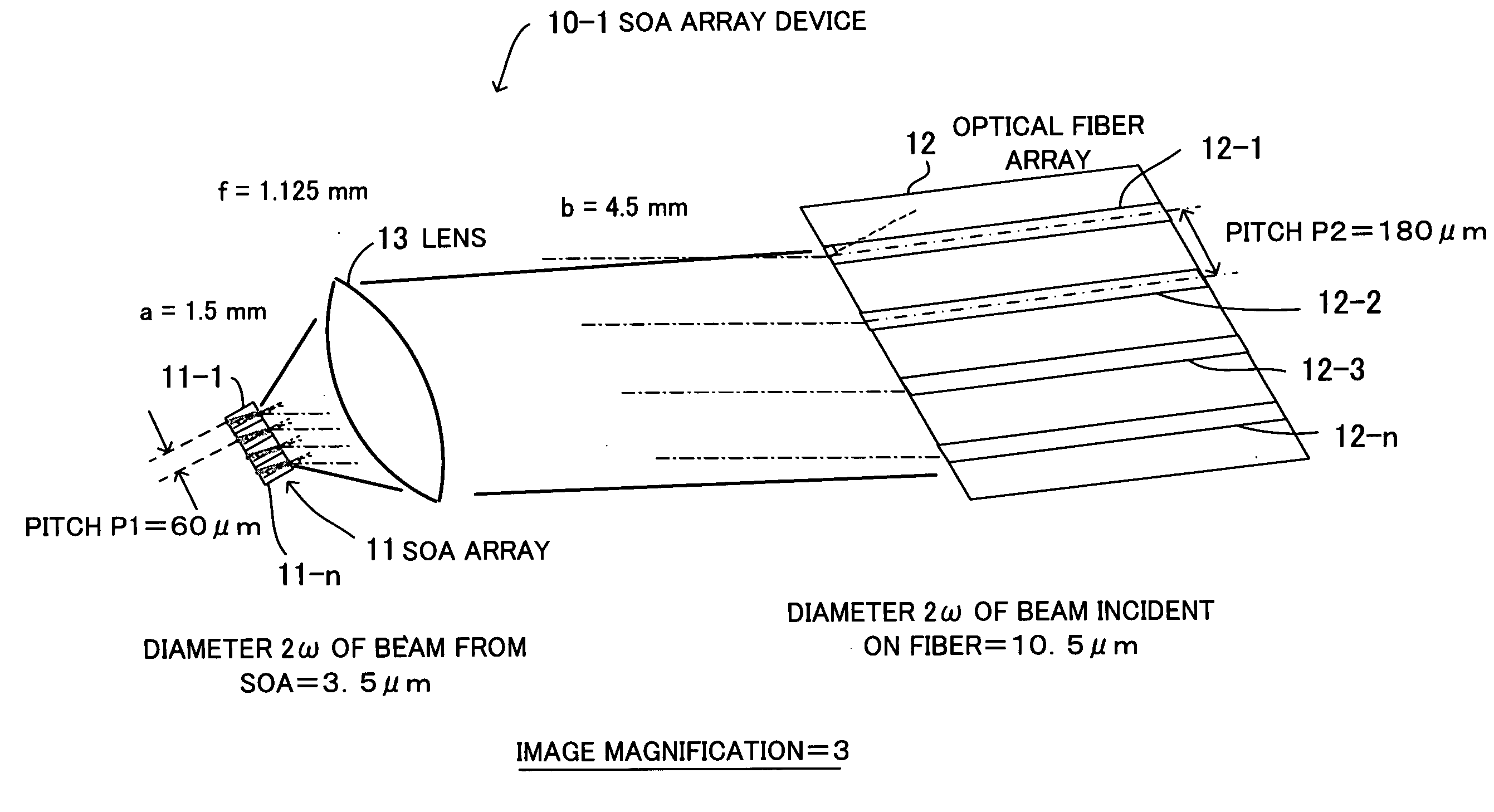
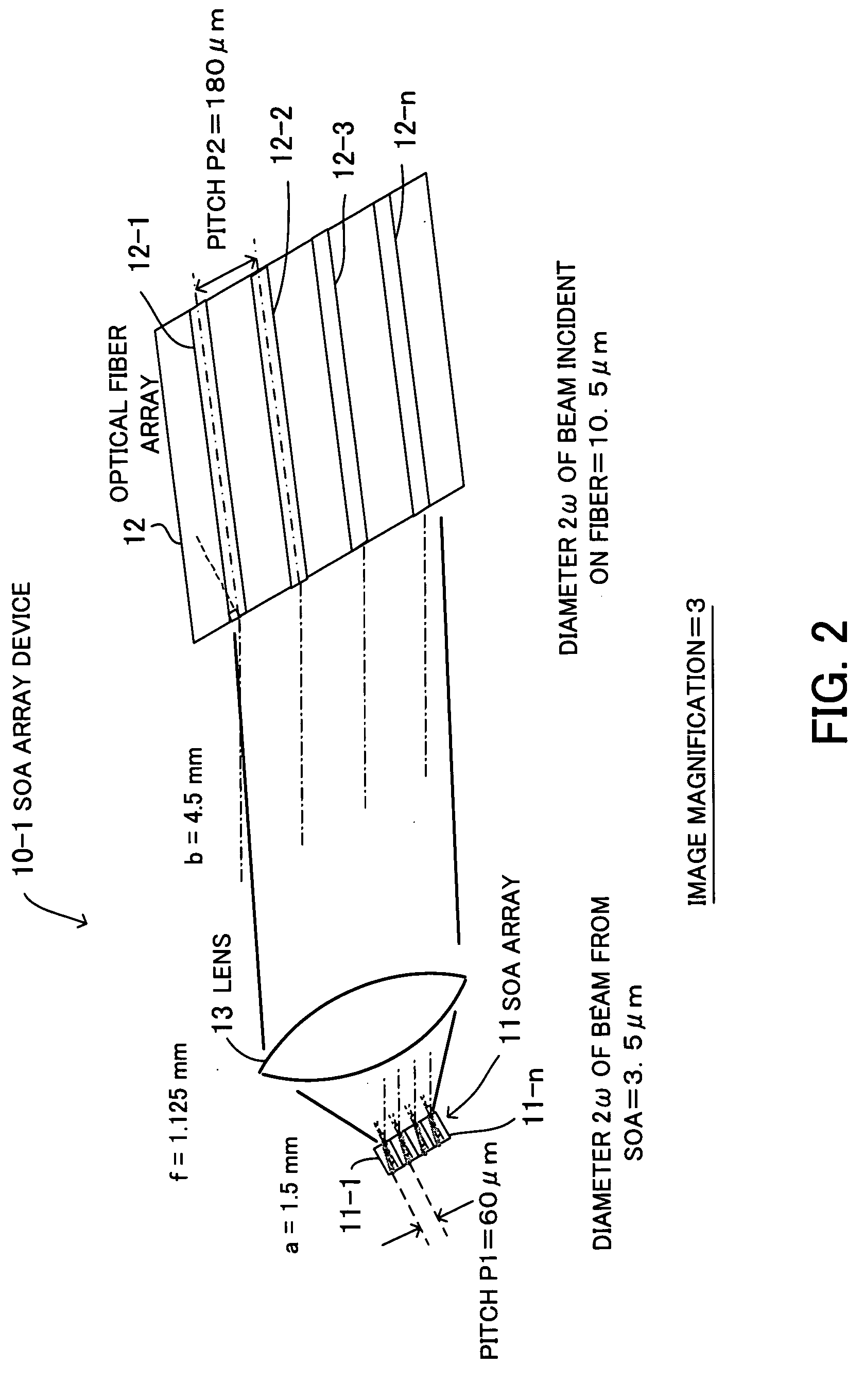
[0052]The following explains the design of the The optical fibers 12-1 to 12-n, which are SMFs (Single Mode Fibers), have a beam diameter of 10.5 μm, and it is assumed that the SOAs 11-1 to 11-n have a beam diameter of 3.5 μm. The beam diameter represents a mode field diameter (MFD), and MFD will be briefly explained with reference to FIG. 3.

[0053]FIG. 3 illustrates MFD, wherein the vertical axis indicates light. intensity and the horizontal axis indicates core diameter. A light beam emerging from an SOA or an optical fiber is not a parallel beam but a radiant beam that radially spreads. MFD is an index representing the degree of such beam spreading relative to the core diameter. The light intensity distribution can be plotted as a curve similar to a Gaussian distribution, as shown in the figure, wherein the light intensity is highest at the center of the core and gradually decreases toward outer regions of the core.

[0054]Provided the maximum light intensity at the center of the co...

second embodiment

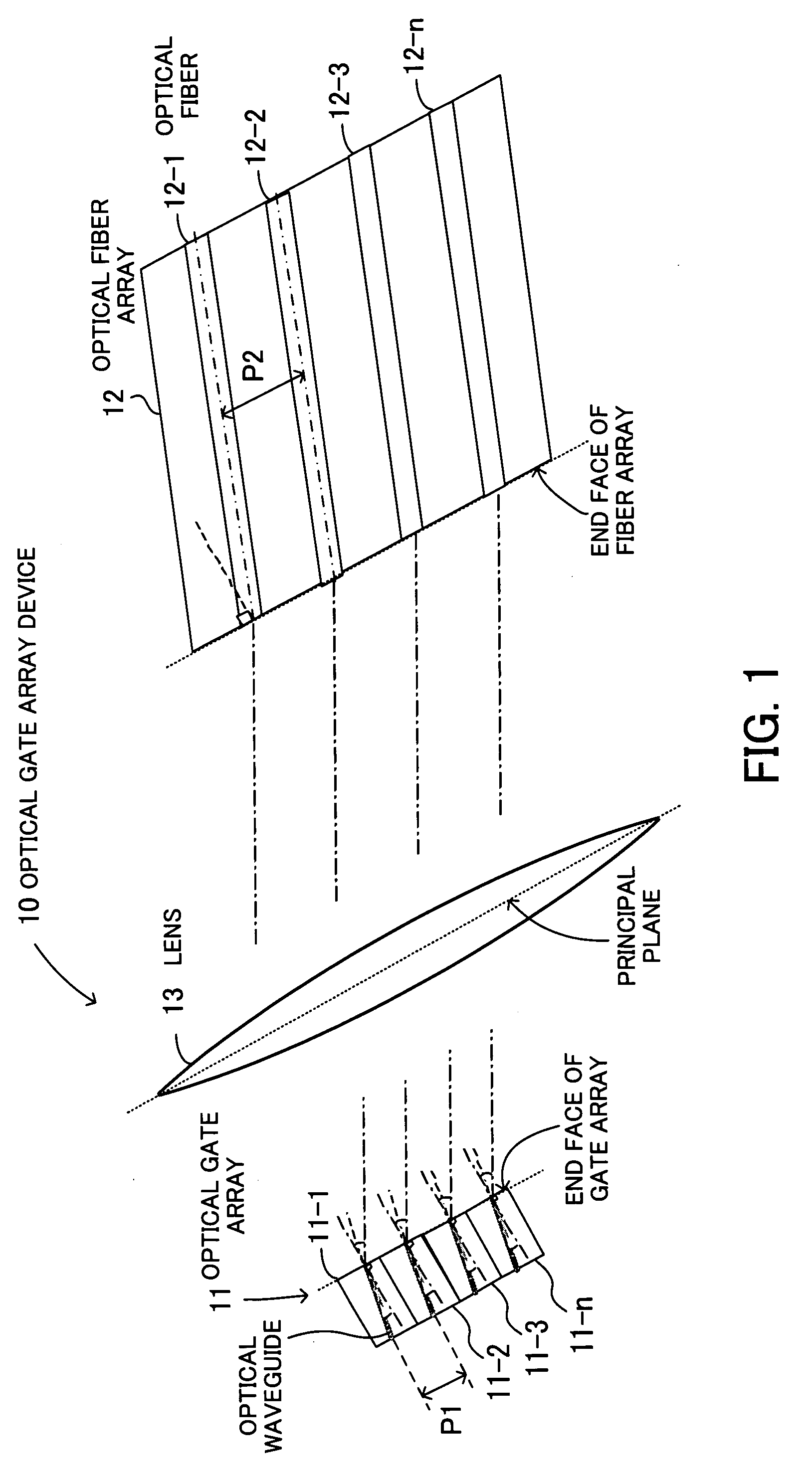
[0069]In the second embodiment, the SOA array 11 and the lens 13-1 constitute a confocal system, and the lens 13-2 and the optical fiber array 12 also constitute a confocal system. The term “confocal” signifies a state in which a light source or a light receiver is arranged at the focus of a lens or a state in which two or more lenses are arranged such that their foci coincide with each other. Accordingly, the SOA array 11 is positioned at the focal point of the lens 13-1, and the optical fiber array 12 is positioned at the focal point of the lens 13-2.

[0070]The overall image magnification of the lenses 13-1 and 13-2 constituting a confocal system is equal to f2 / f1, where f1 is the focal distance of the lens 13-1 and f2 is the focal distance of the lens 13-2. Namely, the distance “a” from the end face of the SOA array 11 to the principal plane of the lens 13-1 is equal to the focal distance “f1” of the lens 13-1, and the distance “b” from the principal plane of the lens 13-2 to the ...


PUM


Abstract

An optical gate array device which permits the use of an optical gate array with a pitch smaller than the diameter of optical fibers. The optical gate array has an array of optical gates, and an optical fiber array has an array of optical fibers. A lens is arranged between the optical gate array and the optical fiber array, for collectively achieving optical coupling between all of the optical gates of the optical gate array and all of the optical fibers of the optical fiber array.

Description

CROSS-REFERENCE TO RELATED APPLICATIONS[0001]This application is based upon and claims the benefits of priority from the prior Japanese Patent Application No. 2006-226552, filed on Aug. 23, 2006, the entire contents of which are incorporated herein by reference.BACKGROUND OF THE INVENTION[0002]1. Field of the Invention[0003]The present invention relates to optical gate array devices, and more particularly, to an optical gate array device having an array of optical gates for controlling optical signals.[0004]2. Description of the Related Art[0005]With the recent increasing demand for broadband communication services, optical communication networks have become capable of carrying a large volume of data over long distances, and the development of high-speed large-capacity WDM (Wavelength Division Multiplex: wavelength division multiplexing technique for multiplexing different wavelengths of light to simultaneously transmit multiple signals over a single optical fiber) has been actively...

Claims


Application Information

Patent Timeline
Patent Type & Authority Applications(United States)
IPC IPC(8): G02B6/32
CPCG02B6/4249G02B6/32
Inventor NAKAGAWA, GOJI
Owner FUJITSU LTD
Why Eureka
Try Eureka