Optical modules

a technology of optical modules and optical components, applied in the field of optical modules, can solve the problems of serious deterioration of the high frequency signal characteristics of the optical module, the total cost of fabricating the optical module,

Active Publication Date: 2014-07-08
ELECTRONICS & TELECOMM RES INST
View PDF24 Cites 11 Cited by
  • Summary
  • Abstract
  • Description
  • Claims
  • Application Information

AI Technical Summary

Benefits of technology

[0005]The present invention provides an optical module for minimizing mismatch of characteristic impedance and improving a high frequency signal characteristic by suppressing high frequency resonances.
[0008]In other embodiments, the optical modules may further include a metal package component surrounding the optical bench having the lens and the semiconductor chip and the flexible printed circuit board to protect them from an external environment.
[0025]In other embodiments of the present invention, optical modules include: a thermo-electric cooler unit; a first optical bench with a lens on the thermo-electric cooler unit; a second optical bench with a trench, contacting on the first optical bench except for a region with the lens; at least one semiconductor chip in the trench of the second optical bench; a flexible printed circuit board covering an upper surface of the second optical bench except for the trench; and a metal package component surrounding the thermo-electric cooler unit, the first optical bench with the lens, the second optical bench with the semiconductor chip, and the flexible printed circuit board to protect them from an external environment, wherein the first and second optical benches are a metal optical bench or a silicon optical bench.
[0026]In still other embodiments of the present invention, optical modules include: a thermo-electric cooler unit; a first optical bench with a lens on the thermo-electric cooler unit; a second optical bench with a trench on the thermo-electric cooler unit, being spaced from the first optical bench; at least one semiconductor chip in the trench of the second optical bench; a flexible printed circuit board covering an upper surface of the second optical bench except for the trench; and a metal package component surrounding the thermo-electric cooler unit, the first optical bench with the lens, the second optical bench with the semiconductor chip, and the flexible printed circuit board to protect them from an external environment, wherein the first and second optical benches are a metal optical bench or a silicon optical bench.

Problems solved by technology

A process for forming the thin-film type termination matching resistor and the via holes on the ceramic submount requires high costs so that it accounts for a significant portion of the total cost for fabricating an optical module.
Generally, if a high frequency signal is connected by bonding wires through a plurality of steps, it is reflected because of characteristic impedance mismatch, so that high frequency signal characteristics of an optical module are seriously deteriorated.

Method used


Image

  • Optical modules
  • Optical modules
  • Optical modules

Examples


Embodiment Construction

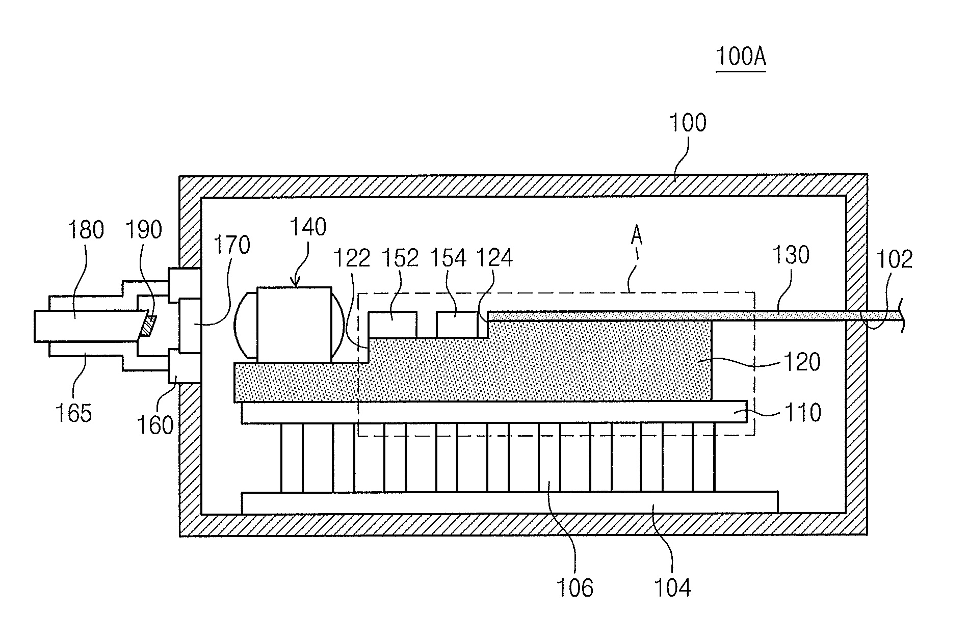
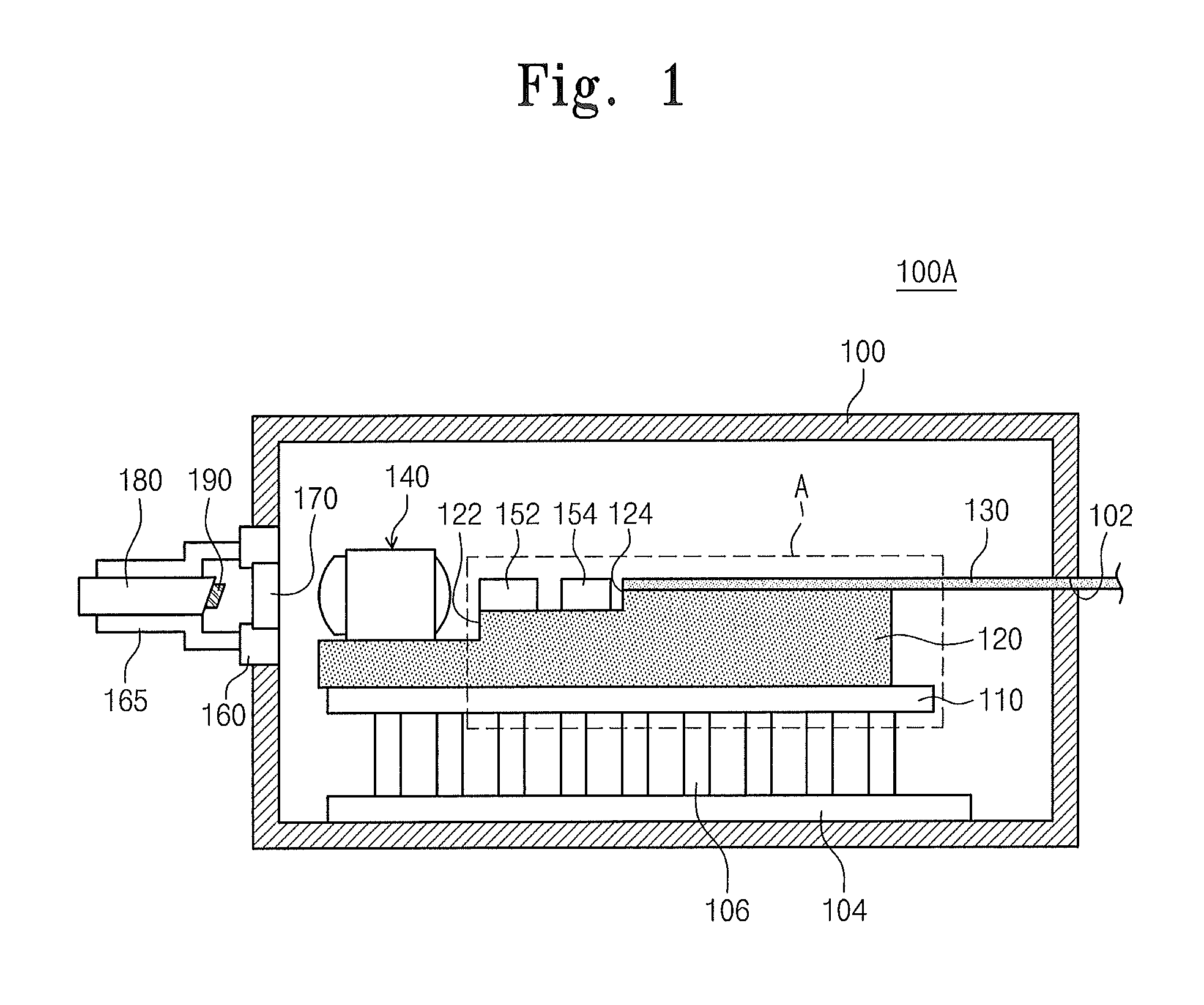
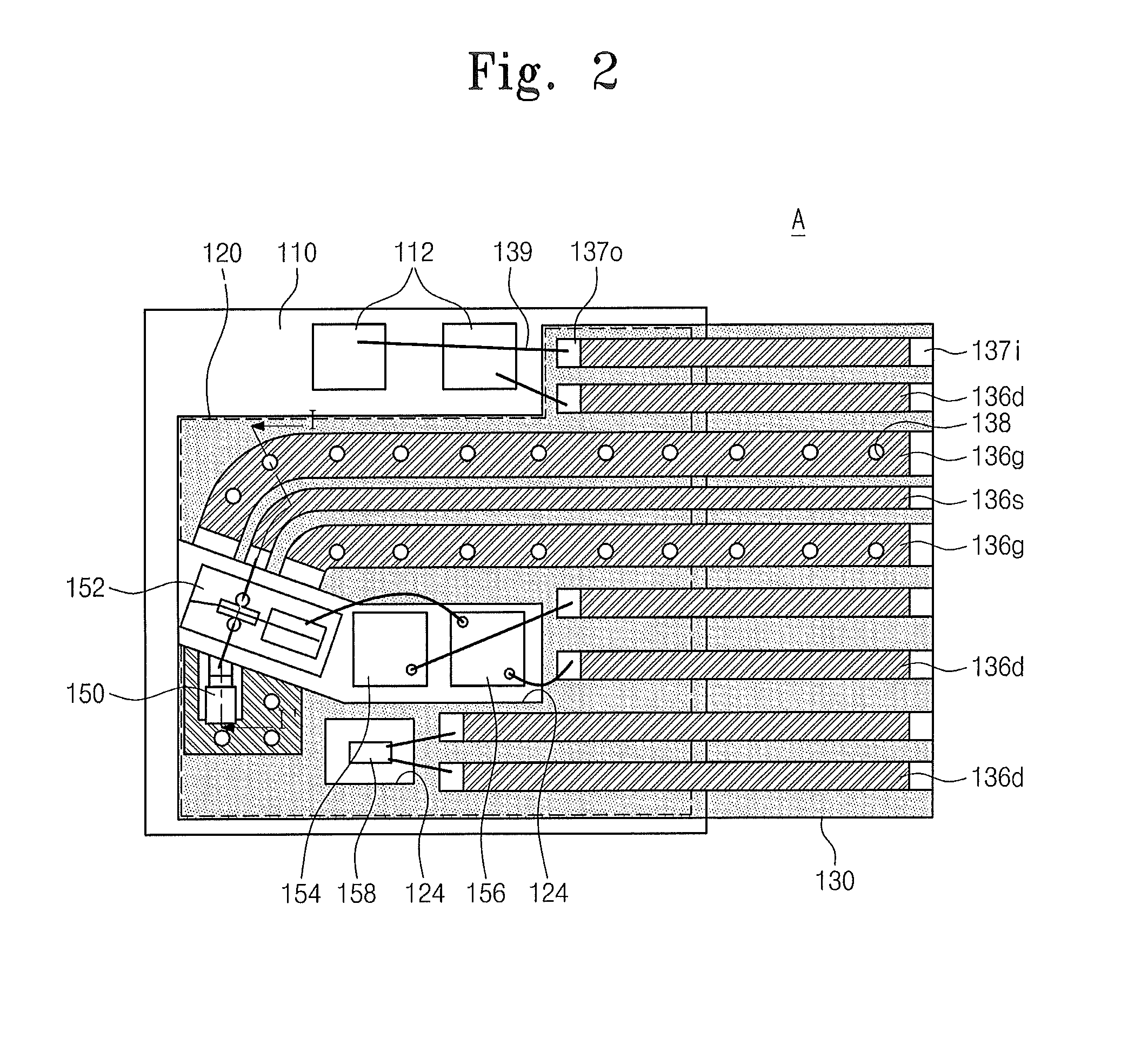
[0034]Preferred embodiments of the present invention will be described below in more detail with reference to the accompanying drawings. Advantages and features of the present invention, and implementation methods thereof will be clarified through following embodiments described with reference to the accompanying drawings. The present invention may, however, be embodied in different forms and should not be construed as limited to the embodiments set forth herein. Rather, these embodiments are provided so that this disclosure will be thorough and complete, and will fully convey the scope of the present invention to those skilled in the art. Further, the present invention is only defined by scopes of claims. Like reference numerals refer to like elements throughout.

[0035]In the following description, the technical terms are used only for explaining specific embodiments while not limiting the present invention. The terms of a singular form may include plural forms unless referred to th...


PUM


Abstract

Provided is an optical module. The optical module includes: an optical bench having a first trench of a first depth and a second trench of a second depth that is less than the first depth; a lens in the first trench of the optical bench; at least one semiconductor chip in the second trench of the optical bench; and a flexible printed circuit board covering an upper surface of the optical bench except for the first and second trenches, wherein the optical bench is a metal optical bench or a silicon optical bench.

Description

CROSS-REFERENCE TO RELATED APPLICATIONS[0001]This U.S. non-provisional patent application claims priority under 35 U.S.C. §119 of Korean Patent Application No. 10-2010-0115478, filed on Nov. 19, 2010, the entire contents of which are hereby incorporated by reference.BACKGROUND OF THE INVENTION[0002]The present invention disclosed herein relates to optical modules, and more particularly, to optical modules for transmitting a high frequency signal.[0003]In order to transmit and process a high frequency signal in a optical transmission or / and optical reception module(s) of more than about 10 Gbps, a ceramic submount is used inside a metal package and a Flexible Printed Circuit Board (FPCB) is used outside the metal package. In the ceramic submount and the FPCB, an electrode of a CoPlanar Waveguide (CPW) form is used. Also, in order to transmit a high frequency signal without reflection, a termination matching resistor is integrated on the ceramic submount with a thin-film type and in o...

Claims


Application Information

Patent Timeline
Patent Type & Authority Patents(United States)
IPC IPC(8): H04B10/00G02B6/12
CPCG02B6/4265G02B6/4281G02B6/4257G02B6/4208G02B6/4271G02B6/4206G02B6/42G02B6/428G02B6/4201G02B6/12002G02B6/12004G02B2006/12092G02B2006/12135G02B6/325G02B6/4279
Inventor HAN, YOUNG-TAKSHIN, JANG UKHAN, SANG-PILPARK, SANG HOBAEK, YONGSOON
Owner ELECTRONICS & TELECOMM RES INST
Why Eureka
Try Eureka