High gain differential amplifier with common-mode feedback

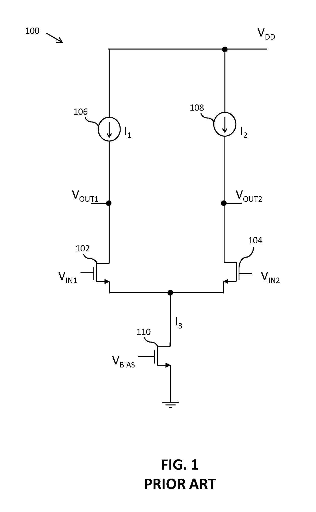
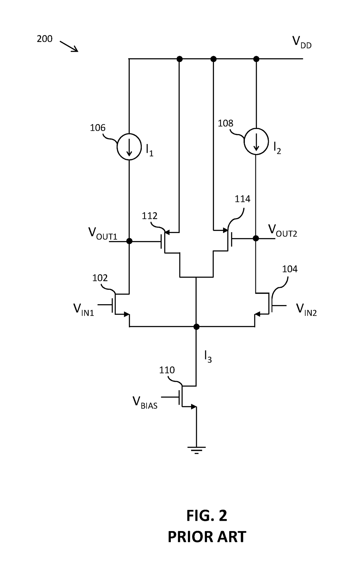
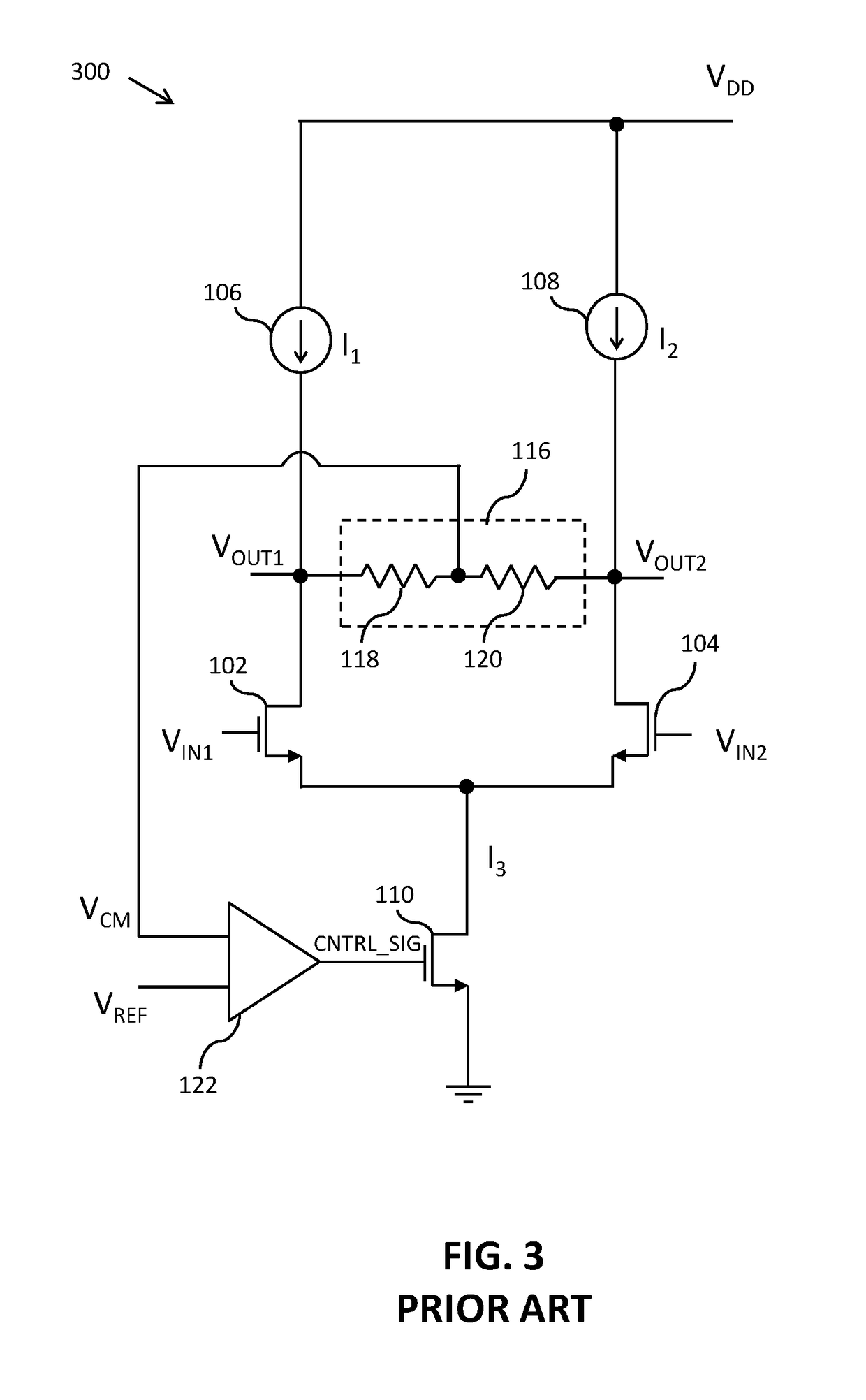
a differential amplifier and common-mode feedback technology, which is applied in the field of integrated circuits, can solve problems such as undesirable, common-mode output voltage of the conventional differential amplifier b>100/b> is susceptible to current mismatch, and differential gain of the differential amplifier b>200/b> is reduced, so as to minimize the mismatch, minimize the mismatch, and minimize the mismatch

Active Publication Date: 2019-03-19
SILICON & BEYOND PVT LTD +1
View PDF4 Cites 2 Cited by
  • Summary
  • Abstract
  • Description
  • Claims
  • Application Information

AI Technical Summary

Benefits of technology

[0012]In an embodiment of the present invention, a high gain differential amplifier with common mode feedback is provided. The high gain differential amplifier includes first through eighth transistors and first through third current sources. A common-mode output voltage of the high gain differential amplifier is controlled by a reference voltage. The first transistor has a gate terminal for receiving the reference voltage and a source terminal connected to the first current source. The first current source receives a supply voltage and outputs a first current. The common-mode output voltage is equal to the reference voltage. The second transistor has a gate terminal connected to a drain terminal thereof and a drain terminal of the first transistor, and a source terminal connected to ground. The third transistor has a gate terminal for receiving a first input voltage, and a drain terminal connected to the second current source. The second current source receives the supply voltage and outputs a second current. The second current flows through the third transistor. The fourth transistor has a gate terminal connected to the drain terminal of the third transistor, a source terminal connected to the source terminal of the first transistor, and a drain terminal connected to a source terminal of the third transistor. The fifth transistor has a gate terminal connected to the third current source, a source terminal connected to the source terminal of the first transistor, and a drain terminal connected to the source terminal of the third transistor. The third current source receives the supply voltage and outputs a third current. The first current flows through the first, fourth, and fifth transistors. The sixth transistor has a gate terminal for receiving a second input voltage, and a drain terminal connected to the gate terminal of the fifth transistor. The common-mode output voltage is measured between the drain terminal of the third transistor and the drain terminal of the sixth transistor. The third current flows through the sixth transistor. The seventh transistor has a gate terminal for receiving a bias voltage, a source terminal connected to the ground, and a drain terminal connected to the source terminal of the third transistor. A fourth current flows through the seventh transistor. The eighth transistor has a gate terminal connected to the gate terminal of the second transistors, a source terminal connected to the ground, and a drain terminal connected to the source terminal of the third transistor. A fifth current flows through the eighth transistor. Further, the fifth current changes proportionally to a mismatch between the fourth current and a sum of second and third current, thereby minimizing the mismatch.
[0013]In another embodiment of the present invention, a high gain differential amplifier with common mode feedback is provided. The high gain differential amplifier includes first through eighth transistors, first through third current sources, and first through third degeneration resistors. A common-mode output voltage of the high gain differential amplifier is controlled by a reference voltage. The first transistor has a gate terminal for receiving the reference voltage and a source terminal connected to a first terminal of the first degeneration resistor. A second terminal of the first degeneration resistor is connected to the first current source. The first current source receives a supply voltage and outputs a first current. The common-mode output voltage is equal to the reference voltage. The second transistor includes a gate terminal connected to a drain terminal thereof and a drain terminal of the first transistor, and a source terminal that receives a ground voltage. The third transistor has a gate terminal that receives a first input voltage, and a drain terminal connected to the second current source. The second current source receives the supply voltage and outputs a second current. The second current flows through the third transistor. The fourth transistor has a gate terminal connected to the drain terminal of the third transistor, a source terminal connected to a first terminal of the second degeneration resistor, and a drain terminal connected to a source terminal of the third transistor. A second terminal of the second degeneration resistor is connected to the first current source. The fifth transistor has a gate terminal connected to the third current source, a source terminal connected to a first terminal of the third degeneration resistor, and a drain terminal connected to the source terminal of the third transistor. The third current source receives the supply voltage and outputs a third current. A second terminal of the third degeneration resistor is connected to the first current source. The first current flows through the first, fourth, and fifth transistors. The sixth transistor has a gate terminal for receiving a second input voltage, and a drain terminal connected to the gate terminal of the fifth transistor. The common-mode output voltage is measured between the drain terminal of the third transistor and the drain terminal of the sixth transistor. The third current flows through the sixth transistor. The seventh transistor has a gate terminal for receiving a bias voltage, a source terminal connected to the ground, and a drain terminal connected to the source terminal of the third transistor. A fourth current flows through the seventh transistor. The eighth transistor has a gate terminal connected to the gate terminal of the second transistor, a source terminal connected to the ground, and a drain terminal connected to the source terminal of the third transistor. A fifth current flows through the eighth transistor. Further, the fifth current changes proportionally to a mismatch between the fourth current and a sum of second and third current, thereby minimizing the mismatch.
[0014]In yet another embodiment of the present invention, a high gain differential amplifier with common mode feedback is provided. The high gain differential amplifier includes first through eighth transistors and first through third current sources. A common-mode output voltage of the high gain differential amplifier is controlled by a reference voltage. The first transistor has a gate terminal for receiving the reference voltage, a source terminal connected to the first current source. The first current source is connected to ground and outputs a first current. The common-mode output voltage is equal to the reference voltage. The second transistor has a gate terminal connected to a drain terminal thereof and a drain terminal of the first transistor, and a source terminal for receiving a supply voltage. The third transistor has a gate terminal for receiving a first input voltage, and a drain terminal connected to the second current source. The second current source is connected to the ground and outputs a second current. The second current flows through the third transistor. The fourth transistor has a gate terminal connected to the drain terminal of the third transistor, a source terminal connected to the source terminal of the first transistor, and a drain terminal connected to a source terminal of the third transistor. The fifth transistor has a gate terminal connected to the third current source, a source terminal connected to the source terminal of the first transistor, and a drain terminal connected to the source terminal of the third transistor. The third current source is connected to the ground and outputs a third current. The first current flows through the first, fourth, and fifth transistors. The sixth transistor has a gate terminal for receiving a second input voltage, and a drain terminal connected to the gate terminal of the fifth transistor. The common-mode output voltage is measured between the drain terminal of the third transistor and the drain terminal of the sixth transistor. The third current flows through the sixth transistor. The seventh transistor has a gate terminal for receiving a bias voltage, a source terminal for receiving the supply voltage, and a drain terminal connected to the source terminal of the third transistor. A fourth current flows through the seventh transistor. The eighth transistor has a gate terminal connected to the gate terminal of the second transistor, a source terminal for receiving the supply voltage, and a drain terminal connected to the source terminal of the third transistor. A fifth current flows through the eighth transistor. Further, the fifth current changes proportionally to a mismatch between the fourth current and a sum of second and third current, thereby minimizing the mismatch.

Problems solved by technology

However, the tail current I3 tends to deviate from the value of the sum of the first and second currents I1 and I2, thereby causing current mismatch.
The common-mode output voltage of the conventional differential amplifier 100 is susceptible to the current mismatch.
In the triode region of operation, differential gain of the differential amplifier 200 reduces which is undesirable.
Furthermore, there is no control over the value of the common-mode output voltage VCM, as the supply voltage signal VDD and gate to source voltage of the PMOS transistor pair VGS cannot be changed frequently as per operational requirements.
Thus, the differential amplifier 300 is highly unreliable and extremely complex to implement.

Method used


Image

  • High gain differential amplifier with common-mode feedback
  • High gain differential amplifier with common-mode feedback
  • High gain differential amplifier with common-mode feedback

Examples


Embodiment Construction

[0024]The detailed description of the appended drawings is intended as a description of the currently preferred embodiments of the present invention, and is not intended to represent the only form in which the present invention may be practised. It is to be understood that the same or equivalent functions may be accomplished by different embodiments that are intended to be encompassed within the spirit and scope of the present invention.

[0025]As used in the specification and claims, the singular forms “a”, “an” and “the” include plural references unless the context clearly dictates otherwise. For example, the term “an article” may include a plurality of articles unless the context clearly dictates otherwise.

[0026]Those with ordinary skill in the art will appreciate that the elements in the figures are illustrated for simplicity and clarity and are not necessarily drawn to scale. For example, the dimensions of some of the elements in the figures may be exaggerated, relative to other ...


PUM


Abstract

A high gain differential amplifier includes first through eighth transistors, first through third degeneration resistors, and first through third current sources. The fourth and fifth transistors form a p-type metal-oxide-semiconductor (PMOS) transistor pair. Further, the second and eighth transistors form a current mirror circuit. The PMOS transistor pair and the current mirror circuit form a common mode feedback circuit. The high gain differential amplifier controls the common-mode output voltage with the common mode feedback circuit and a reference voltage.

Description

CROSS-RELATED APPLICATIONS[0001]This application claims priority of Indian non-provisional Application Serial No. 201741015555, filed May 3, 2017, the contents of which are incorporated herein by reference.FIELD OF THE INVENTION[0002]The present invention relates generally to integrated circuits, and more specifically to differential amplifiers.DESCRIPTION OF THE RELATED ART[0003]Differential circuits are widely used for designing mixed-signal systems due to their ability to effectively reject ambient noise signals in the mixed-signal systems. Examples of the ambient noise signals include supply noise, reference noise, substrate noise, and the like. The ambient noise signals distort input and output signals in circuit implementations of the mixed-signal systems. A differential amplifier is one such circuit implementation of the differential circuits.[0004]Referring now to FIG. 1, a conventional differential amplifier 100 is shown. The conventional differential amplifier 100 is opera...

Claims


Application Information

Patent Timeline
Patent Type & Authority Patents(United States)
IPC IPC(8): H03F3/45H03F3/72
CPCH03F3/45183H03F3/45237H03F3/72H03F3/45475H03F3/45273H03F3/4565H03F2203/45406H03F2203/45418H03F2203/45424H03F2203/45482
Inventor WADEKAR, JAYESHMEHTA, RAVICHATTOPADHYAY, BIMAN
Owner SILICON & BEYOND PVT LTD
Why Eureka
Try Eureka