Semiconductor memory device for minimizing mismatch of sense amplifier

a memory device and semiconductor technology, applied in semiconductor devices, digital storage, instruments, etc., can solve problems such as inability to operate semiconductor devices normally, invalid sensing, or invalid data sensing, and achieve the effect of minimizing mismatch

Active Publication Date: 2014-01-28
SK HYNIX INC
View PDF13 Cites 0 Cited by
  • Summary
  • Abstract
  • Description
  • Claims
  • Application Information

AI Technical Summary

Benefits of technology

[0016]Various embodiments of the technique described herein minimize mismatch between transistors which operate in pair in a sense amplifier.
[0017]According to one aspect of an embodiment, a semiconductor memory device may include a sense amplifier and a buffer. The sense amplifier senses and amplifies a difference between signals of a bit line pair. The sense amplifier may include PMOS transistors and NMOS transistors, and may be a cross-coupled latch type sense amplifier. The buffer prevents mismatch, and may be formed between the PMOS transistors and the NMOS transistors.

Problems solved by technology

However, invalid sensing, or sensing of invalid data, may occur in cross-coupled latch type sense amplifier when there is mismatch of a threshold voltage between components (for example, transistors) of the sense amplifier.
Thus, when mismatch occurs between transistors that form one or more of the pairs, the semiconductor device does not normally operate.
Thus, a mismatch may result when concentrations of impurities implanted into the active regions are different in an impurity implantation process.

Method used


Image

  • Semiconductor memory device for minimizing mismatch of sense amplifier
  • Semiconductor memory device for minimizing mismatch of sense amplifier
  • Semiconductor memory device for minimizing mismatch of sense amplifier

Examples


Embodiment Construction

”.

BRIEF DESCRIPTION OF THE DRAWINGS

[0024]The above and other aspects, features and other advantages of the subject matter of the present disclosure will be more clearly understood from the following detailed description taken in conjunction with the accompanying drawings.

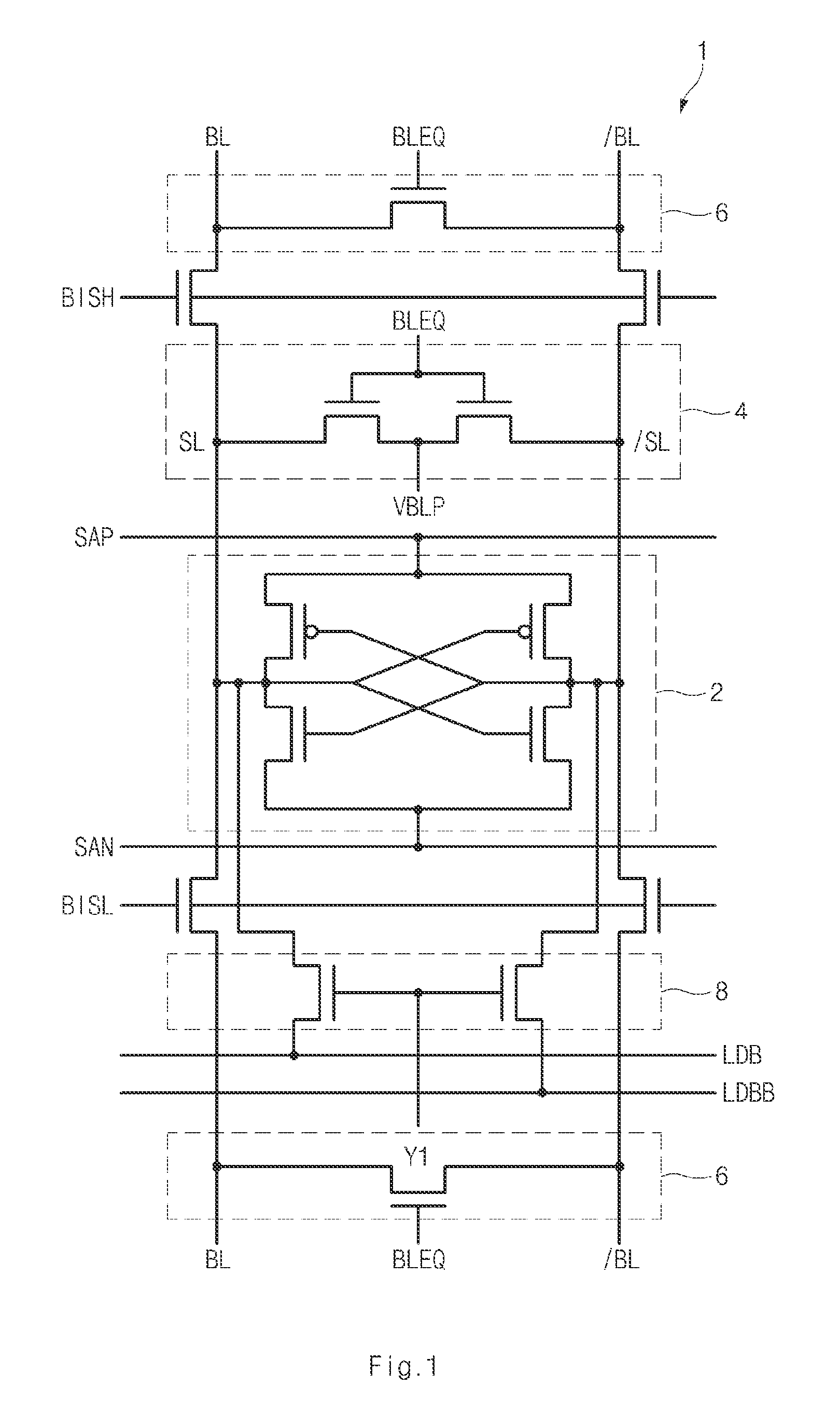
[0025]FIG. 1 is a circuit diagram illustrating a configuration of a general cross-coupled latch type sense amplifier unit corresponding to a folded type bit line structure.

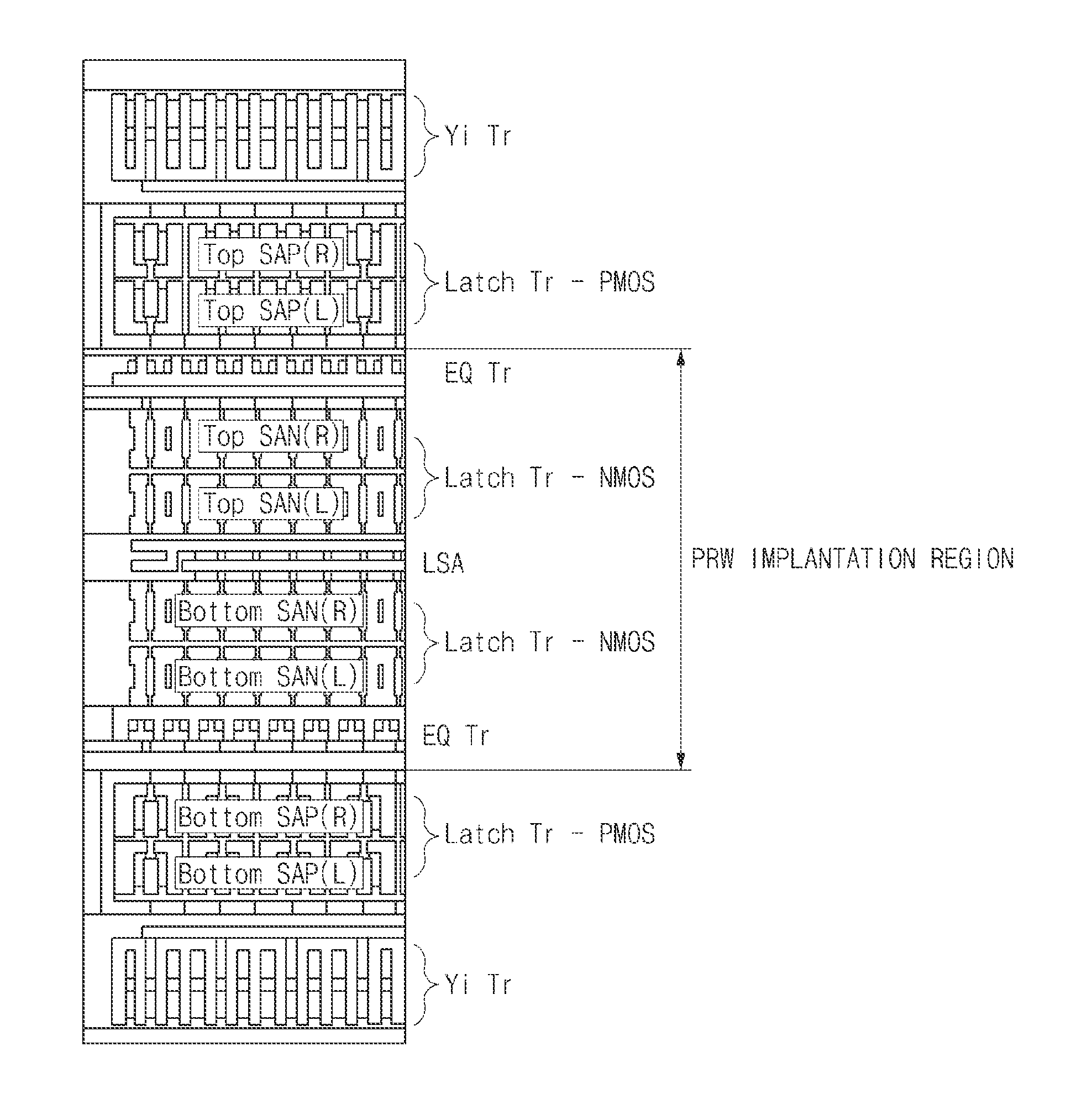
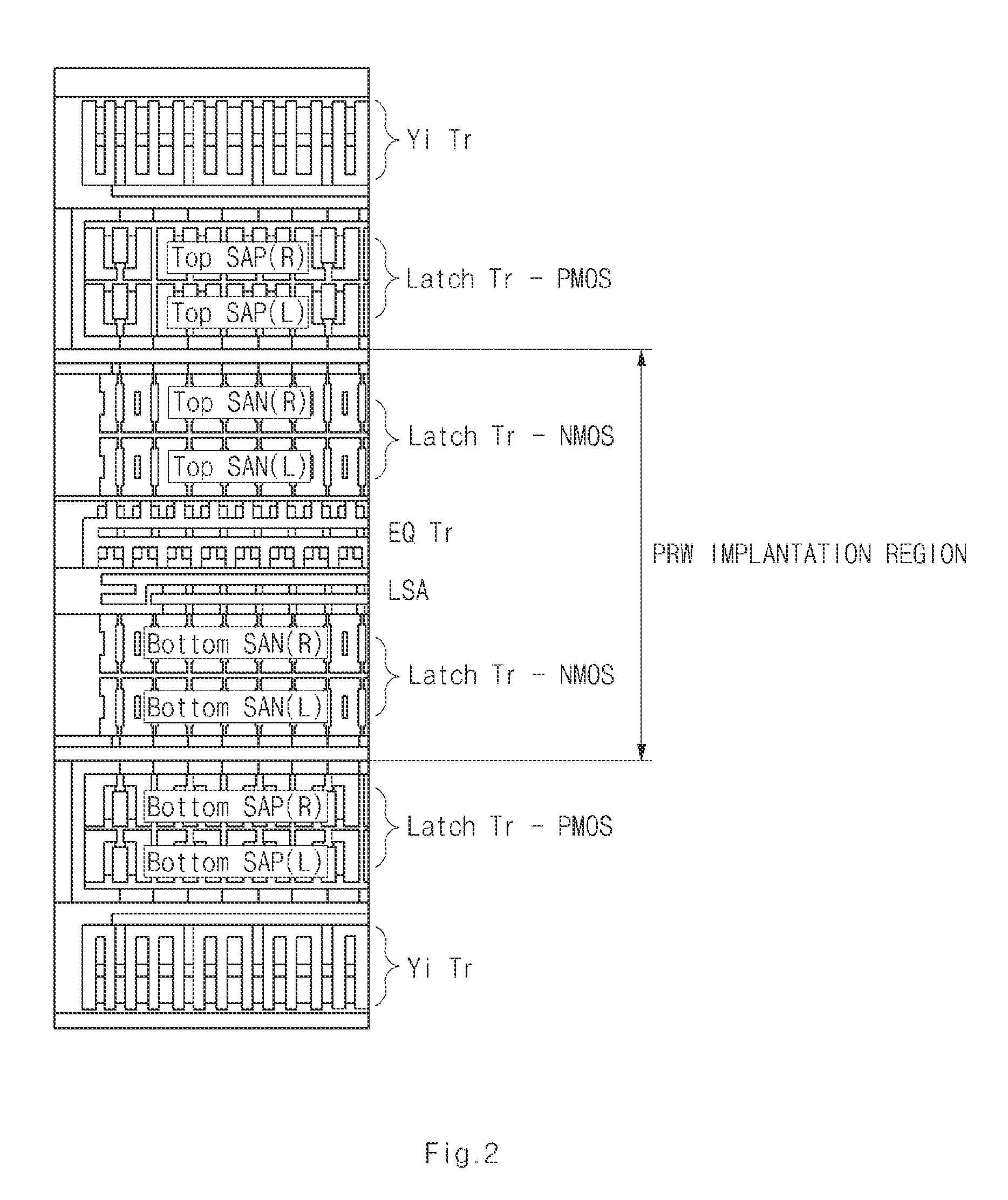
[0026]FIG. 2 is a plan view illustrating a substantial layout of a sense amplifier formed in a second generation double data rate type three (2G DDR3) memory device having a 6F2 structure.

[0027]FIG. 3 is a plan view illustrating a layout of a sense amplifier according to an embodiment of the inventive concept.

[0028]FIG. 4 is a view illustrating a relationship between a photoresist (PR) covering a PMOS transistor region and NMOS transistors in the sense amplifier having the layout of FIG. 3.

DESCRIPTION OF EXEMPLARY EMBODIMENTS

[0029]Exemplary embodi...


PUM


Abstract

A semiconductor memory device is provided. The semiconductor memory device includes a cross-coupled latch type sense amplifier and a buffer that prevents mismatch. The buffer is formed between PMOS transistors and NMOS transistors of the sense amplifier so that mismatch for transistors operating in pair can be minimized.

Description

CROSS-REFERENCES TO RELATED APPLICATION[0001]The present application claims priority to Korean patent application number 10-2011-0015620, filed on 22 Feb. 2011, which is incorporated by reference in its entirety.BACKGROUND OF THE INVENTION[0002]1. Technical Field[0003]The inventive concept relates to a semiconductor memory device, and more particularly, to a semiconductor memory device capable of minimizing mismatch of transistors which operate in pairs in a sense amplifier.[0004]2. Related Art[0005]Semiconductor memory devices generally include bit line sense amplifiers which sense and amplify data stored in memory cells.[0006]A method of sensing by a general sense amplifier is by differential pair sensing. The most commonly used sense amplifier is a cross-coupled latch type sense amplifier.[0007]However, invalid sensing, or sensing of invalid data, may occur in cross-coupled latch type sense amplifier when there is mismatch of a threshold voltage between components (for example, t...

Claims


Application Information

Patent Timeline
Patent Type & Authority Patents(United States)
IPC IPC(8): G11C7/06
CPCG11C7/065H01L27/0207G11C11/4091H01L27/092G11C7/06G11C11/4094
Inventor KOO, DONG, CHUL
Owner SK HYNIX INC
Why Eureka
Try Eureka