Supercharge Your Innovation With Domain-Expert AI Agents!

Method for making light emitting diode

a technology of light-emitting diodes and methods, applied in the direction of basic electric elements, electrical equipment, semiconductor devices, etc., can solve the problems of low extraction efficiency and degrading extraction efficiency of leds

Active Publication Date: 2014-07-29
TSINGHUA UNIV +1
View PDF9 Cites 0 Cited by
  • Summary
  • Abstract
  • Description
  • Claims
  • Application Information

AI Technical Summary

Benefits of technology

The present patent text is about a new LED and a method for making it. The LED has a high extraction efficiency, meaning it can convert electrical energy into light more effectively than previous LEDs. The LED has a three-dimensional structure, including a N-type semiconductor layer, a P-type semiconductor layer, an active layer, an N-type electrode, and a P-type electrode. The method for making the LED involves forming a three-dimensional array of nanostructures in the active layer. The LED has a contact area between the N-type semiconductor layer and the active layer that is not large enough, resulting in low electron-hole recombination density and sparse photons. The patent aims to overcome these shortcomings and improve the extraction efficiency of LEDs.

Problems solved by technology

However, the extraction efficiency of LEDs is low because the contact area between the N-type semiconductor layer and the active layer is not large enough.
Thus the electron-hole recombination density is low, and the photons in the LED are sparse, thereby degrading the extraction efficiency.

Method used


Image

  • Method for making light emitting diode
  • Method for making light emitting diode
  • Method for making light emitting diode

Examples


Embodiment Construction

[0019]The disclosure is illustrated by way of example and not by way of limitation in the figures of the accompanying drawings in which like references indicate similar elements. It should be noted that references to “an” or “one” embodiment in this disclosure are not necessarily to the same embodiment, and such references mean at least one.

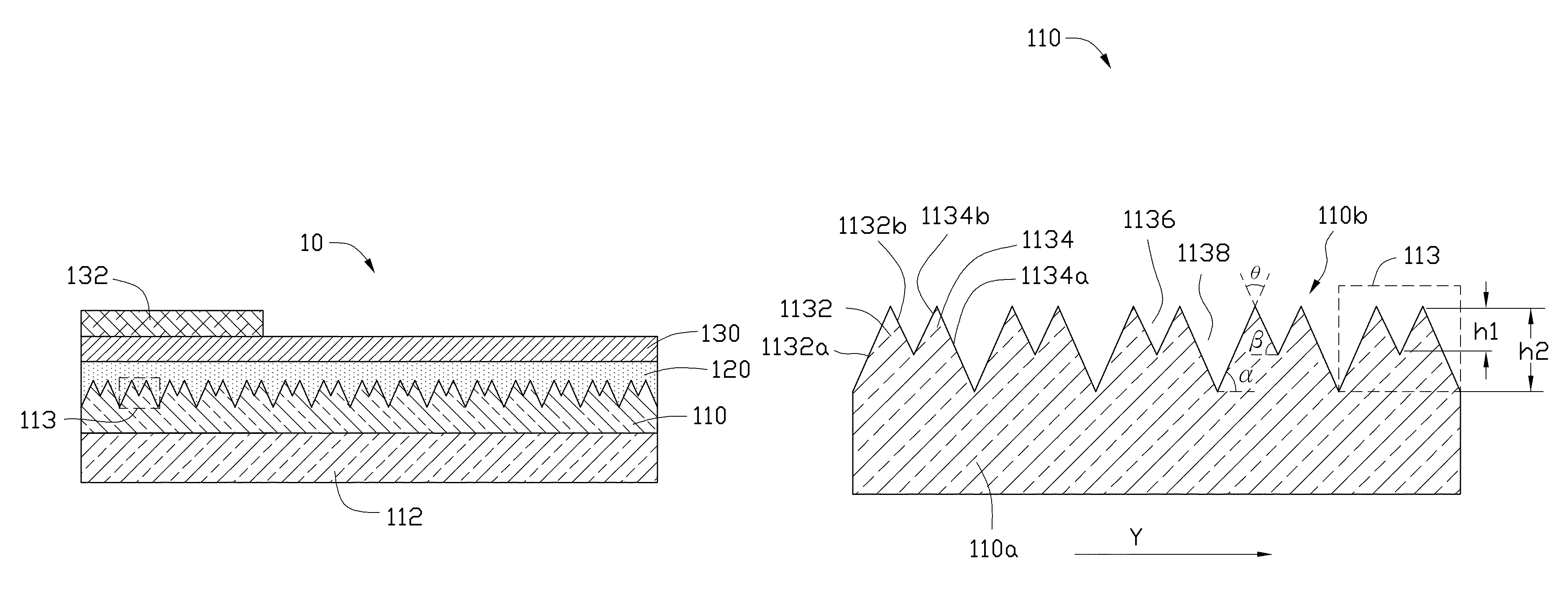
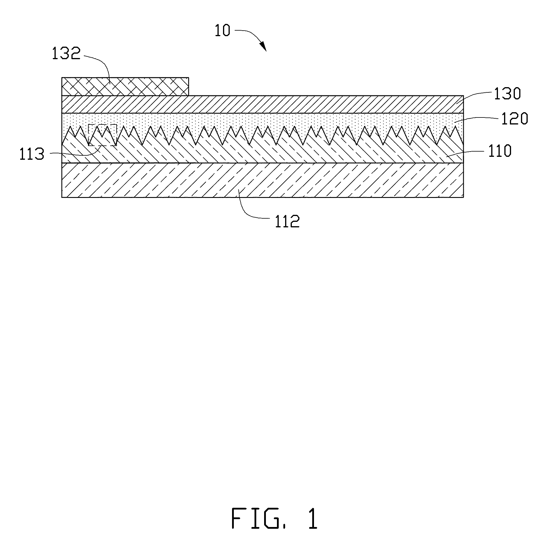
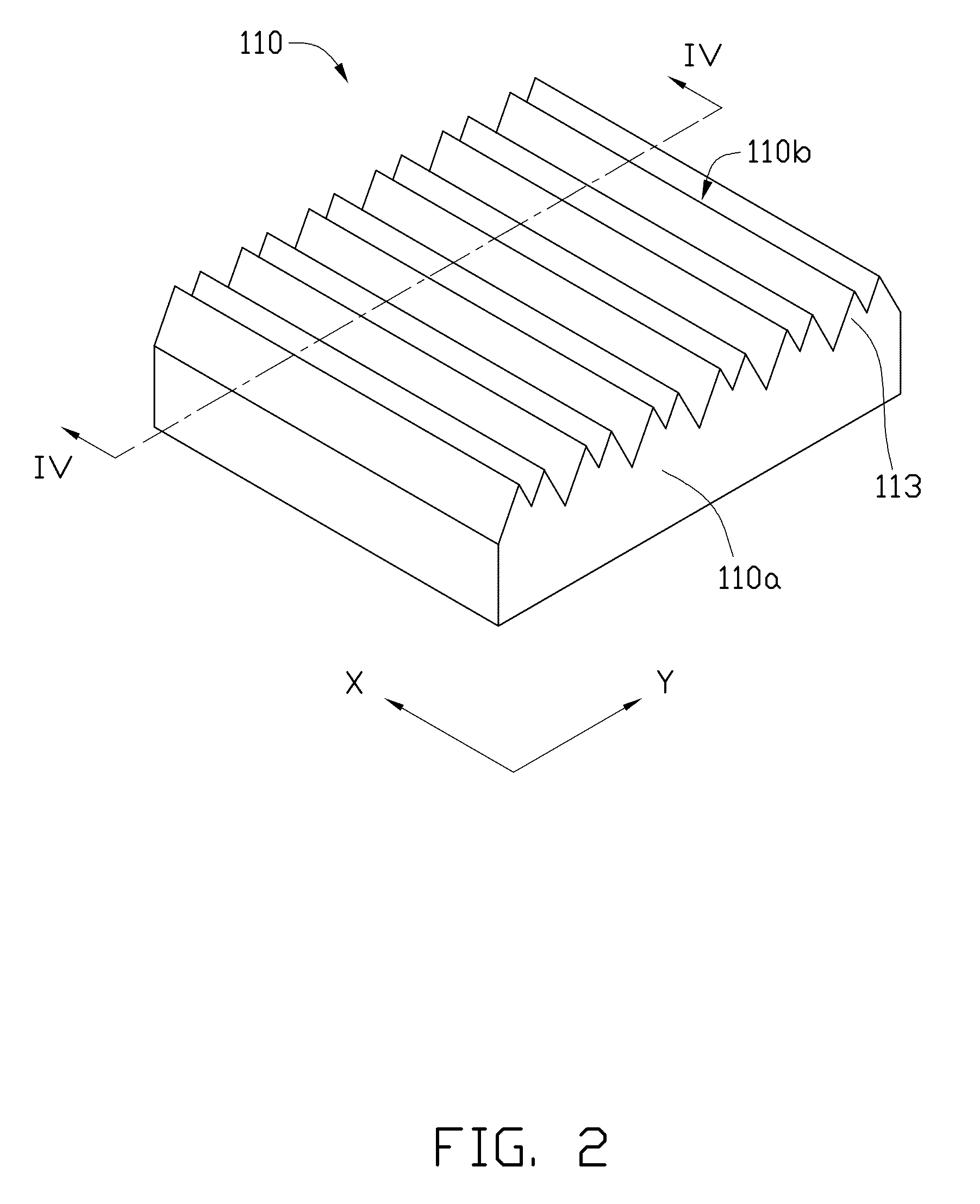
[0020]Referring to FIG. 1, an LED 10 includes a first semiconductor layer 110, an active layer 120, a second semiconductor layer 130, a first electrode 112, and a second electrode 132. The first semiconductor layer 110 defines a plurality of three-dimensional nano-structures 113. The active layer 120 is sandwiched between the first semiconductor layer 110 and the second semiconductor layer 130. The first semiconductor layer 110 includes a first surface and a second surface opposite to the first surface. The active layer 120 and the second semiconductor layer 130 are stacked on the second surface of the first semiconductor layer 110. The first ele...


PUM


Abstract

A method for making light emitting diode includes the following steps. A substrate is provided. A first semiconductor layer is grown on a surface of the substrate. A patterned mask layer is located on a surface of the first semiconductor layer, and the patterned mask layer includes a number of bar-shaped protruding structures, a slot is defined between each two adjacent protruding structures to expose a portion of the first semiconductor layer. The exposed first semiconductor layer is etched to form a protruding pair. A number of three-dimensional nano-structures are formed. An active layer and a second semiconductor layers are grown on the number of three-dimensional nano-structures in that order. The substrate is removed and a surface of the first semiconductor layer is exposed. A first electrode is applied to cover the exposed surface. A second electrode is electrically connected with the second semiconductor layer.

Description

CROSS-REFERENCE TO RELATED APPLICATIONS[0001]This application claims all benefits accruing under 35 U.S.C. §119 from China Patent Application No. 201110395474.7, filed on Dec. 3, 2011 in the China Intellectual Property Office, disclosure of which is incorporated herein by reference. This application is related to applications entitled, “LIGHT EMITTING DIODE”, filed May 23, 2012 Ser. No. 13 / 479,223; “LIGHT EMITTING DIODE”, filed May 23, 20012 Ser. No. 13 / 479,225; “LIGHT EMITTING DIODE”, filed May 23, 2012 Ser. No. 13 / 479,227; “METHOD FOR MAKING LIGHT EMITTING DIODE”, filed May 23, 2012 Ser. No. 13 / 479,229; “LIGHT EMITTING DIODE”, filed May 23, 2012 Ser. No. 13 / 479,230; “LIGHT EMITTING DIODE”, filed May 23, 2012 Ser. No. 13 / 479,233; “METHOD FOR MAKING LIGHT EMITTING DIODE”, filed May 23, 2012 Ser. No. 13 / 479,234; “LIGHT EMITTING DIODE”, filed May 22, 2012 Ser. No. 13 / 477,273.BACKGROUND[0002]1. Technical Field[0003]The present disclosure relates to a light emitting diode (LED) and the ...

Claims


Application Information

Patent Timeline
Patent Type & Authority Patents(United States)
IPC IPC(8): H01L21/00H01L33/00
CPCH01L33/0079H01L21/0237H01L21/0242H01L21/02458H01L21/02513H01L21/0254H01L21/0262H01L21/02658H01L33/005H01L33/24H01L33/0093
Inventor ZHU, ZHEN-DONGLI, QUN-QINGZHANG, LI-HUICHEN, MOFAN, SHOU-SHAN
Owner TSINGHUA UNIV
Features
  • R&D
  • Intellectual Property
  • Life Sciences
  • Materials
  • Tech Scout
  • Unparalleled Data Quality
  • Higher Quality Content
  • 60% Fewer Hallucinations
Learn More