MOS transistor with forward bulk-biasing circuit

a transistor and bulk biasing technology, applied in the field of electronic circuits, can solve the problems of exponential increase in leakage current, degrading performance, and increasing power consumption of transistors

Active Publication Date: 2014-08-12
NXP USA INC
View PDF20 Cites 10 Cited by
  • Summary
  • Abstract
  • Description
  • Claims
  • Application Information

AI Technical Summary

Problems solved by technology

Although, reduced transistor size leads to a direct design benefit of increased processing power, it also leads to a design trade-off by increasing power consumption of the transistors and hence, that of the ICs.
However a reduction in the supply voltage Vdd decreases the processing, thereby degrading performance.
However, a reduction in the threshold voltage Vth of the trans...

Method used


Image

  • MOS transistor with forward bulk-biasing circuit
  • MOS transistor with forward bulk-biasing circuit
  • MOS transistor with forward bulk-biasing circuit

Examples


Embodiment Construction

[0010]The detailed description of the appended drawings is intended as a description of the currently preferred embodiments of the present invention, and is not intended to represent the only form in which the present invention may be practiced. It is to be understood that the same or equivalent functions may be accomplished by different embodiments that are intended to be encompassed within the spirit and scope of the present invention.

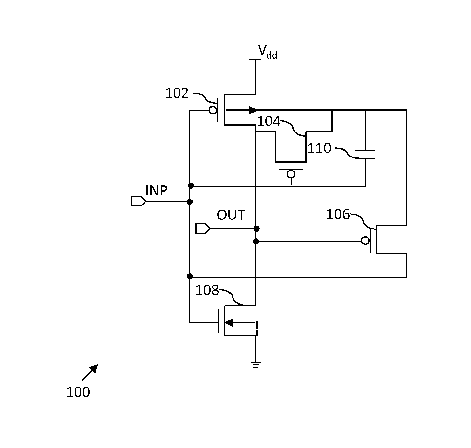
[0011]In an embodiment of the present invention, a forward bulk-biasing circuit is provided. The forward bulk-biasing circuit includes a first transistor having a source terminal for receiving a supply voltage and a gate terminal for receiving an input signal; a second transistor having a drain terminal connected to a bulk terminal of the first transistor for forward bulk-biasing the bulk terminal, a source terminal connected to a drain terminal of the first transistor, and a gate terminal connected to the gate terminal of the first transistor for re...


PUM


Abstract

Forward bulk biasing circuitry for PMOS and NMOS transistors is provided. The bulk biasing circuitry includes two N-type MOS transistors, two P-type MOS transistors, and two capacitors. The forward bias to a bulk terminal of a transistor increases a threshold voltage of a transistor, thereby reducing a transition time and improving the performance of the transistor. The forward bias is provided only when the transistor transitions from one state to another, thereby reducing leakage power dissipation during active and standby modes of an integrated circuit that includes the transistor.

Description

BACKGROUND OF THE INVENTION[0001]The present invention relates generally to electronic circuits, and more specifically, to a MOS transistor with a forward bulk-biasing circuit.[0002]Recent years have witnessed an increased demand for small, high-performance electronic devices. This demand has been addressed primarily with the evolution of integrated circuits (ICs) designed using very large scale integration (VLSI). Using VLSI, electronic circuits may by designed by combining hundreds of thousands of transistors onto a single IC. This is achieved by miniaturizing transistors to sizes on the order of about 50 nanometer (nm) or less. Integrating large numbers of transistors on a single chip has successfully enabled design of small electronic devices with high processing power.[0003]Although, reduced transistor size leads to a direct design benefit of increased processing power, it also leads to a design trade-off by increasing power consumption of the transistors and hence, that of the...

Claims


Application Information

Patent Timeline
IPC IPC(8): G05F5/00G05F3/20H03K19/00H03K3/01
CPCH03K19/0027G05F5/00G05F3/205
Inventor ROY, AMITDEY, AMIT KUMARMISRI, KULBHUSHANTAYAL, VIJAYVERMA, CHETAN
Owner NXP USA INC
Why Eureka
Try Eureka