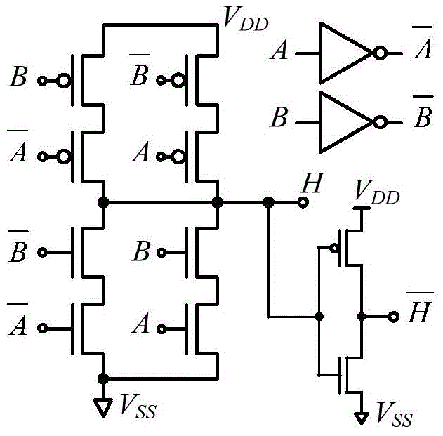
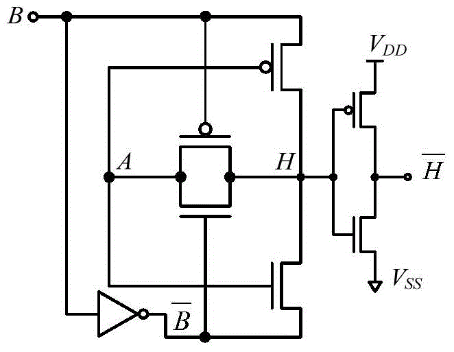
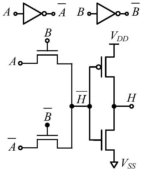
Grid voltage bootstrapping xor/xnor circuit and grid voltage bootstrapping single-bit full adder
A gate voltage bootstrap and full adder technology, applied in the field of XOR circuit, can solve the problems of threshold voltage loss, power consumption-delay product, etc., to reduce leakage power consumption, improve performance, and increase operation speed effect
- Summary
- Abstract
- Description
- Claims
- Application Information
AI Technical Summary
Problems solved by technology
Method used
Image
Examples
Embodiment 1
[0025] Example 1: as Figure 9As shown, a gate voltage bootstrap XOR / OR circuit includes a gate voltage bootstrap XOR generation circuit and an inverter, and the gate voltage bootstrap XOR generation circuit includes a first PMOS tube, a second PMOS tube, a first PMOS tube, and a second PMOS tube. An NMOS tube, a second NMOS tube, a third NMOS tube and a fourth NMOS tube, the inverter includes a third PMOS tube and a fifth NMOS tube, the source of the first PMOS tube is connected to the positive pole of the external power supply, the first PMOS tube The drain of the tube is connected to the source of the second PMOS tube, the gate of the first PMOS tube is connected to the source of the first NMOS tube and the source of the third NMOS tube respectively, and the substrate of the second PMOS tube is connected to the external power supply The anode of the second PMOS tube is connected to the source of the second NMOS tube and the source of the fourth NMOS tube respectively, the d...
Embodiment 2
[0027] Embodiment 2: The rest is the same as Embodiment 1, the difference is the channel length of the first PMOS tube, the channel length of the second PMOS tube, the channel length of the third PMOS tube, and the channel length of the fourth PMOS tube. Channel length, channel length of the fifth PMOS transistor, channel length of the sixth PMOS transistor, channel length of the seventh PMOS transistor, channel length of the first NMOS transistor, channel length of the second NMOS transistor, third The channel length of the NMOS transistor, the channel length of the fourth NMOS transistor, the channel length of the fifth NMOS transistor, the channel length of the sixth NMOS transistor, the channel length of the seventh NMOS transistor, the channel length of the eighth NMOS transistor The length and the channel length of the ninth NMOS transistor under the PTM90nm standard process are both 90nm.
Embodiment 3
[0028] Embodiment 3: The rest is the same as Embodiment 1, the difference is the channel length of the first PMOS tube, the channel length of the second PMOS tube, the channel length of the third PMOS tube, and the channel length of the fourth PMOS tube. Channel length, channel length of the fifth PMOS transistor, channel length of the sixth PMOS transistor, channel length of the seventh PMOS transistor, channel length of the first NMOS transistor, channel length of the second NMOS transistor, third The channel length of the NMOS transistor, the channel length of the fourth NMOS transistor, the channel length of the fifth NMOS transistor, the channel length of the sixth NMOS transistor, the channel length of the seventh NMOS transistor, the channel length of the eighth NMOS transistor The length and the channel length of the ninth NMOS transistor under the PTM45nm standard process are both 50nm.
[0029] In order to compare the gate voltage bootstrap XOR / XOR circuit proposed i...
PUM
 Abstract
Description
Claims
Application Information


