Integrated system on chip using multiple MEMS and CMOS devices
What is AI technical title?
AI technical title is built by Patsnap AI team. It summarizes the technical point description of the patent document.
a technology of integrated systems and cmos, applied in the field of integrated devices, can solve the problems of increasing the cost of cmos devices, focusing on mems development, and ics and in particular mems still have limitations, and achieve the effects of reducing off-chip connections, reducing costs, and being convenient to us
Active Publication Date: 2014-09-02
MOVELLA INC
View PDF174 Cites 16 Cited by
Summary
Abstract
Description
Claims
Application Information
AI Technical Summary
This helps you quickly interpret patents by identifying the three key elements:
Problems solved by technology
Method used
Benefits of technology
Benefits of technology
[0010]Many benefits are achieved by way of the present invention over conventional techniques. For example, the present techniques provide easy to use processes that rely upon conventional fabrication technologies. In some embodiments, the methods provide higher device yields in dies per wafer as a result of the integrated approach. Also, the methods provide processes and systems that are compatible with conventional process technologies without substantial modifications to conventional equipment and processes. Various embodiments of these techniques can reduce off-chip connections, which make the mass production of smaller and thinner units possible. Additionally, various embodiments of the integrated CMOS-MEMS technologies described herein can achieve high accuracy through the minimization or reduction of parasitic resistances and capacitances due to joint (e.g. simultaneous) fabrication of CMOS and MEMS devices, and in particular, CMOS and multiple (e.g. different) MEMS devices.
Problems solved by technology
Although highly successful, ICs and in particular MEMS still have limitations.
Similar to IC development, MEMS development, which focuses on increasing performance, reducing size, and decreasing cost, continues to be challenging.
Additionally, applications of MEMS often require increasingly complex microsystems that desire greater computational power.
Unfortunately, such applications generally do not exist.
Method used
Image
Click on the blue label to locate the original text in one second.
Reading with bidirectional positioning of images and text.
Examples
Embodiment Construction
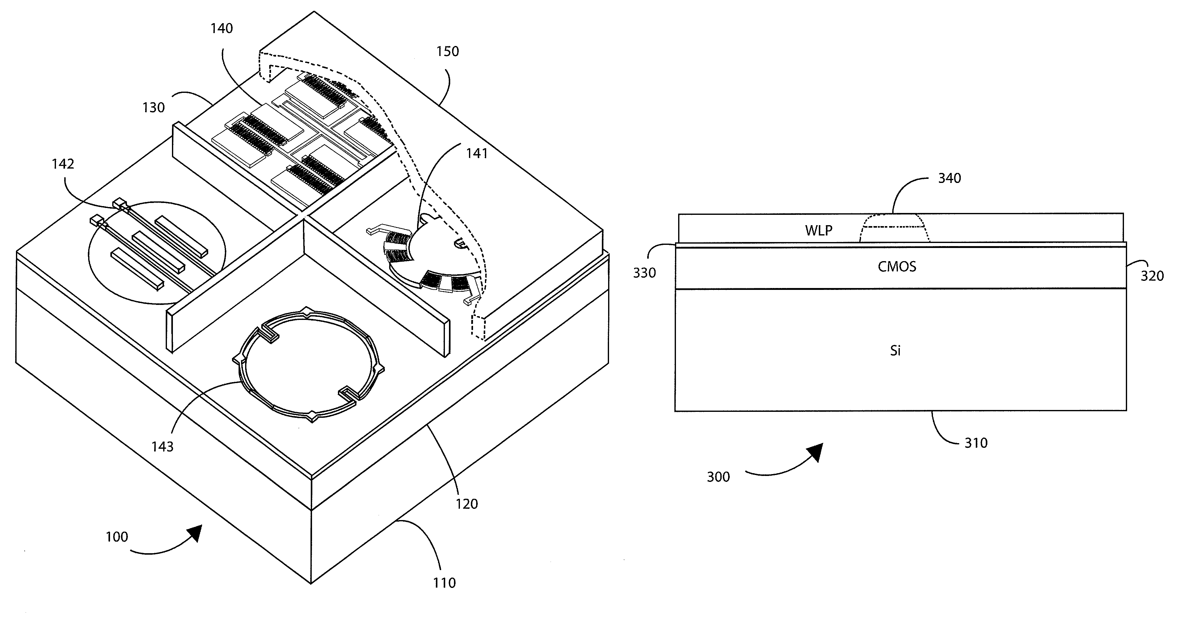
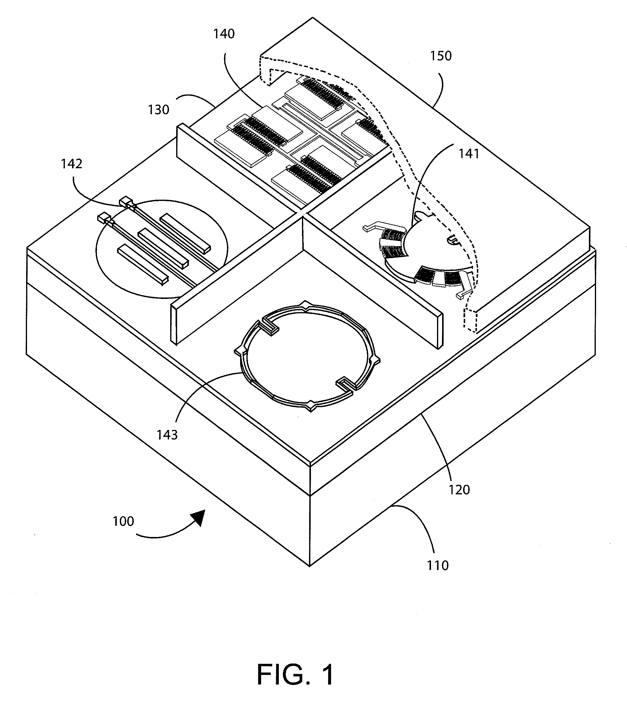
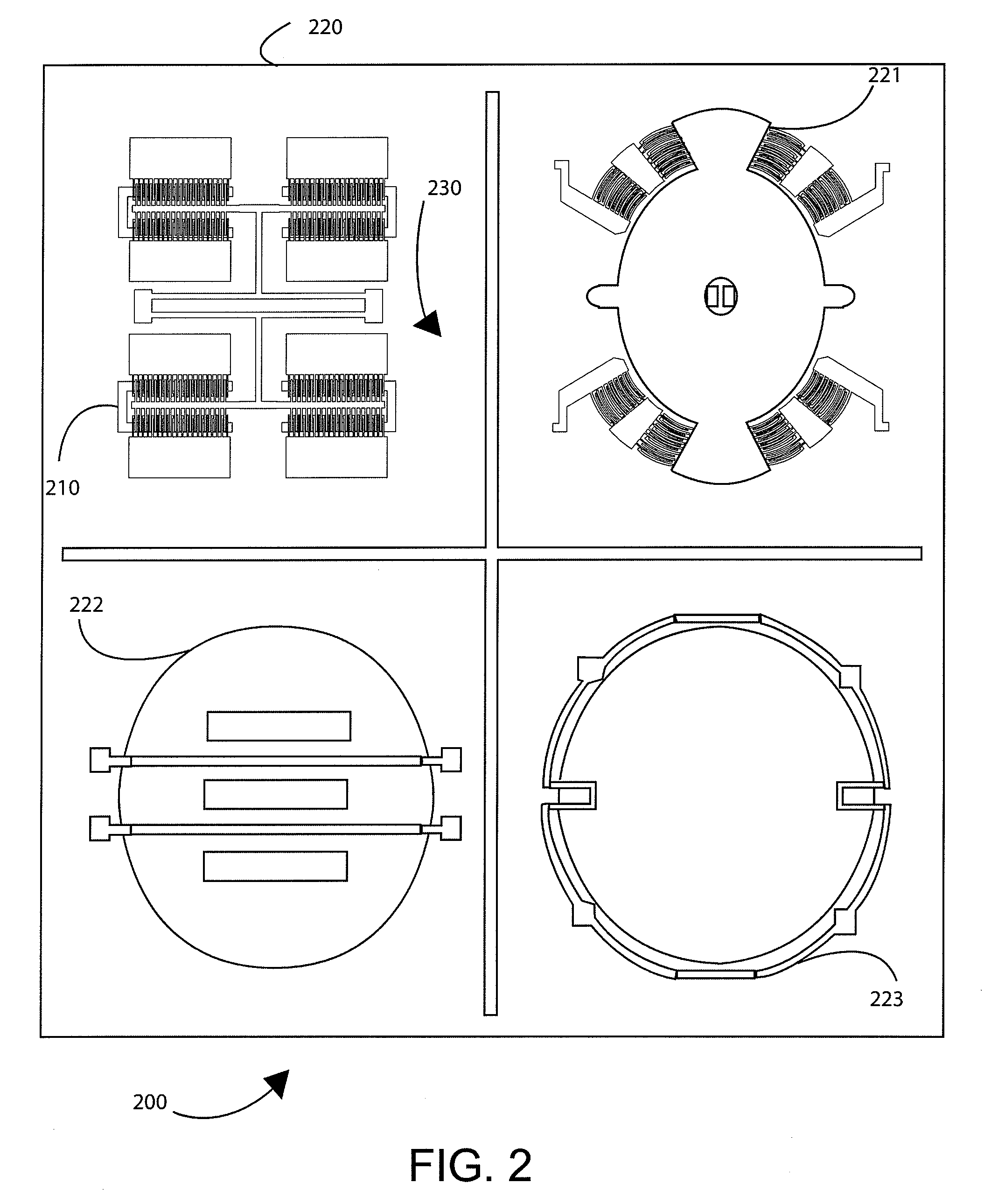
[0028]According to the present invention, techniques related generally to integrated devices and systems are provided. More particularly, the present invention provides systems and methods for integrating one or more MEMS devices with other system applications configured on at least CMOS integrated circuit devices. Merely by way of example, the MEMS devices can include at least an accelerometer, a gyroscope, a magnetic sensor, a pressure sensor, a microphone, a humidity sensor, a temperature sensor, a chemical sensor, a biosensor, an inertial sensor, and others. Additionally, the other applications include at least a sensor application or applications, system applications, and broadband applications, among others. But it will be recognized that the invention has a much broader range of applicability.
[0029]FIG. 1 is a simplified perspective diagram of an integrated CMOS-MEMS system according to an embodiment of the present invention. This diagram is merely an example, which should no...
PUM
Abstract
An integrated MEMS System. CMOS and MEMS devices can be provided in order to form an integrated CMOS-MEMS system. The system can include a silicon substrate layer, a CMOS layer, MEMS and CMOS devices, and a wafer level packaging (WLP) layer. The CMOS layer can form an interface region, one which any number of CMOS MEMS devices can be configured. The integrated MEMS devices can include, but not exclusively, an combination of the following types of sensors: magnetic, pressure, humidity, temperature, chemical, biological, or inertial. Furthermore, the overlying WLP layer can be configured to hermetically seal any number of these integrated devices. The present technique provides an easy to use process that relies upon conventional process technology without substantial modifications to conventional equipment and process and reduces off-chip connections, which make the mass production of smaller and thinner units possible.
Description
CROSS-REFERENCE TO RELATED APPLICATIONS[0001]The present application claims priority to and incorporates by reference, for all purposes, the following patent application: Provisional Application No. 61 / 255,490, filed Oct. 28, 2009. The present invention also incorporates by reference, for all purposes, the following patent applications related to sensor and MEMS devices: U.S. patent application Ser. No. 12 / 859,631, filed Aug. 19, 2010, Provisional Application No. 61 / 356,467, filed Jun. 18, 2010, U.S. patent application Ser. No. 12 / 859,672, filed Aug. 19, 2010, and U.S. patent application Ser. No. 12 / 859,647, filed Aug. 19, 2010.BACKGROUND OF THE INVENTION[0002]The present invention relates generally to integrated devices. More particularly, the present invention provides a system and method for integrating at least two different micro electro mechanical systems (MEMS) devices with one or more complementary metal oxide semiconductor (CMOS) devices, but can be others. Merely by way of...
Claims
Application Information
Patent Timeline
Application Date:The date an application was filed.
Publication Date:The date a patent or application was officially published.
First Publication Date:The earliest publication date of a patent with the same application number.
Issue Date:Publication date of the patent grant document.
PCT Entry Date:The Entry date of PCT National Phase.
Estimated Expiry Date:The statutory expiry date of a patent right according to the Patent Law, and it is the longest term of protection that the patent right can achieve without the termination of the patent right due to other reasons(Term extension factor has been taken into account ).
Invalid Date:Actual expiry date is based on effective date or publication date of legal transaction data of invalid patent.

