Organic light emitting display device and method for manufacturing the same

a technology of light-emitting diodes and display devices, which is applied in the direction of semiconductor devices, electrical devices, transistors, etc., can solve the problems of deterioration of the whole characteristics of the organic light-emitting diodes (oled) display, and achieve the effect of suppressing the generation of deterioration

Inactive Publication Date: 2014-09-02
SAMSUNG DISPLAY CO LTD
View PDF9 Cites 0 Cited by
  • Summary
  • Abstract
  • Description
  • Claims
  • Application Information

AI Technical Summary

Benefits of technology

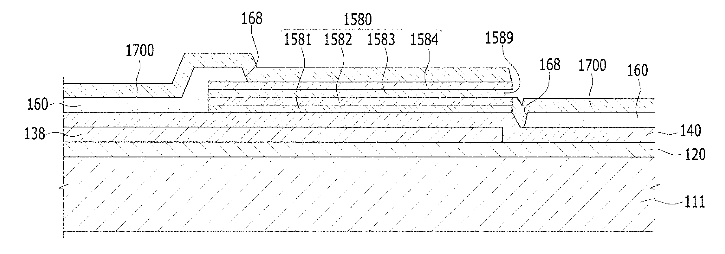
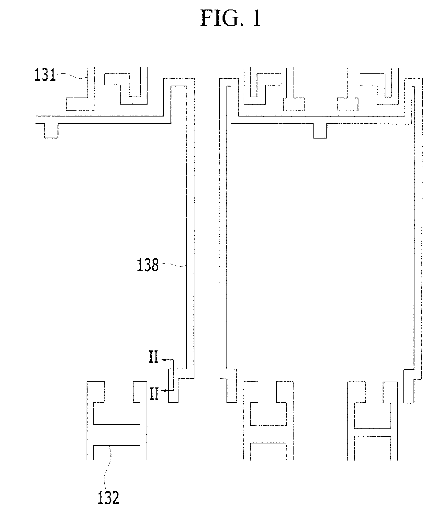
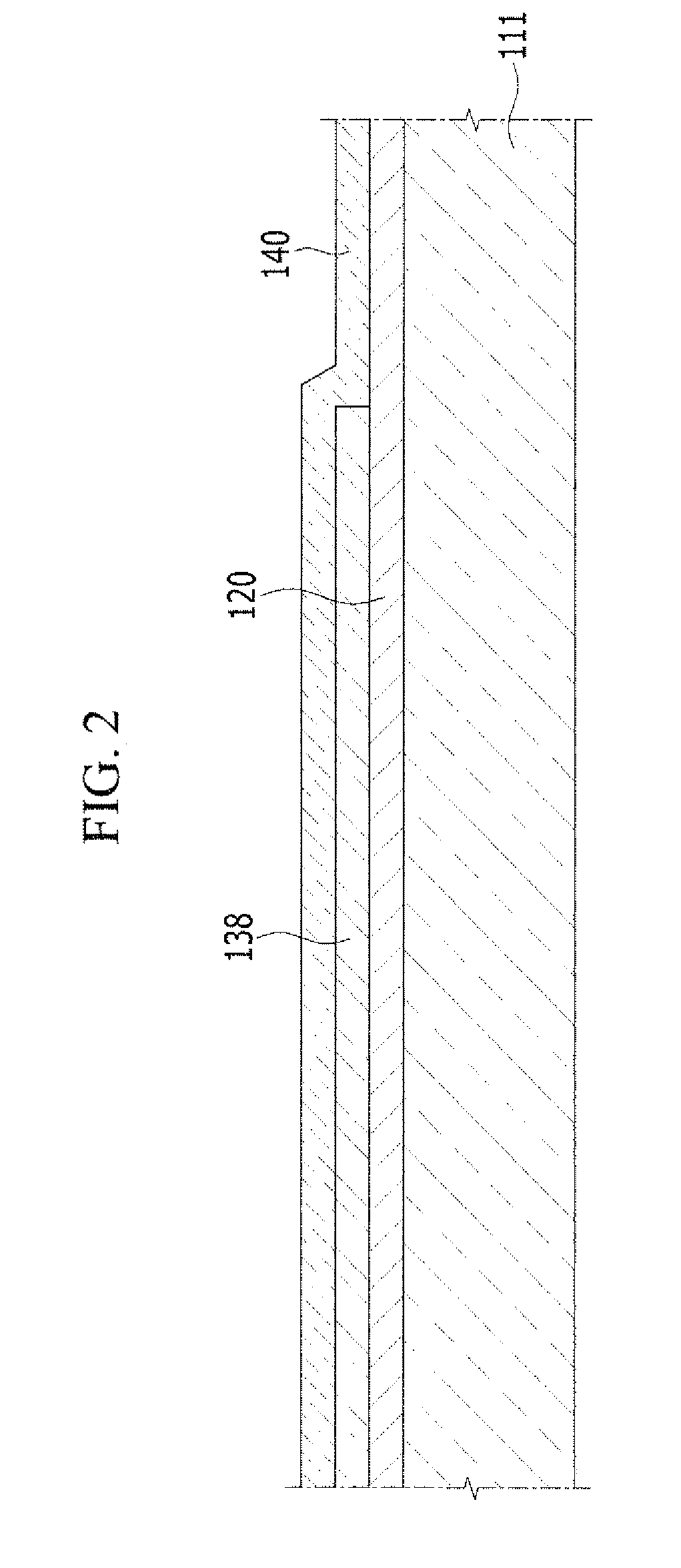
[0009]An exemplary embodiment provides an organic light emitting diode (OLED) display suppressing generation of deterioration due to non-doping of an impurity at a portion of a semiconductor layer used as one electrode of a capacitor.
[0027]At least one metal layer among the plurality of metal layers except for the highest layer may be relatively more easily eroded by the hydrofluoric acid solution than the highest layer.
[0031]According to an exemplary embodiment, the organic light emitting diode (OLED) display may suppress deterioration generated by one region where the impurity is doped in the semiconductor layer that is used as one electrode of the capacitor.

Problems solved by technology

However, if the impurity is not doped to a portion of the semiconductor layer used as one electrode of the capacitor by a limitation of a manufacturing process, the whole characteristics of the organic light emitting diode (OLED) display are deteriorated.

Method used


Image

  • Organic light emitting display device and method for manufacturing the same
  • Organic light emitting display device and method for manufacturing the same
  • Organic light emitting display device and method for manufacturing the same

Examples


Embodiment Construction

[0052]The present invention will be described more fully hereinafter with reference to the accompanying drawings, in which exemplary embodiments of the invention are shown. As those skilled in the art would realize, the described embodiments may be modified in various different ways, all without departing from the spirit or scope of the present invention.

[0053]The drawings and description are to be regarded as illustrative in nature and not restrictive. Like reference numerals designate like elements throughout the specification. In addition, herein, the first exemplary embodiment will be mainly described, and other exemplary embodiments will be primarily described with regard to configurations other than those of the first exemplary embodiment.

[0054]In addition, the size and thickness of each component shown in the drawings are arbitrarily shown for understanding and ease of description, but the present invention is not limited thereto. In the drawings, the thickness of layers, fil...


PUM


Abstract

In an organic light emitting diode (OLED) display and a manufacturing method, an organic light emitting diode (OLED) display includes: a substrate; a semiconductor layer pattern formed on the substrate and including a first capacitor electrode; a gate insulating layer covering the semiconductor layer pattern; a first conductive layer pattern formed on the gate insulating layer and including a second capacitor electrode having at least a portion overlapping the first capacitor electrode; an interlayer insulating layer having a capacitor opening exposing a portion of the second capacitor electrode and covering the second capacitor electrode; and a second conductive layer pattern formed on the interlayer insulating layer, wherein the capacitor opening includes a first transverse side wall parallel to and overlapping the second capacitor electrode, a second transverse side wall parallel to and not overlapping the second capacitor electrode, and a longitudinal side wall connecting the first transverse side wall and the second transverse side wall to each other and overlapping the first capacitor electrode.

Description

CLAIM OF PRIORITY[0001]This application makes reference to, incorporates the same herein, and claims all benefits accruing under 35 U.S.C. §119 from an application earlier filed in the Korean Intellectual Property Office on the 25th of Nov. 2010 and there duly assigned Serial No. 10-2010-0118334.BACKGROUND OF THE INVENTION[0002]1. Field of the Invention[0003]The present invention relates generally to an organic light emitting diode (OLED) display having a semiconductor layer used as one electrode of a capacitor, and a manufacturing method thereof.[0004]2. Description of the Related Art[0005]An organic light emitting diode (OLED) display has been paid much attention as a next-generation display because of its merits such as a wide viewing angle, a fast response rate, and relatively less power consumption, as well as a lesser weight and a slim size.[0006]The organic light emitting diode (OLED) display includes a thin film transistor, an organic light emitting element, and a capacitor....

Claims


Application Information

Patent Timeline
Patent Type & Authority Patents(United States)
IPC IPC(8): H01L29/12H01L29/786
CPCH01L27/3265H01L27/1222H10K59/1216
Inventor PARK, SUNPARK, JONG-HYUNLEE, YUL-KYUKIM, DAE-WOO
Owner SAMSUNG DISPLAY CO LTD
Why Eureka
Try Eureka