Organic light-emitting diode and method for manufacturing same
a light-emitting diode and organic technology, applied in the field of organic light-emitting diodes, can solve the problems of significant reduction of light-emitting efficiency, achieve the effects of simple and economical manufacturing process, enhance the efficiency of excitons, and facilitate the transfer of holes
- Summary
- Abstract
- Description
- Claims
- Application Information
AI Technical Summary
Benefits of technology
Problems solved by technology
Method used
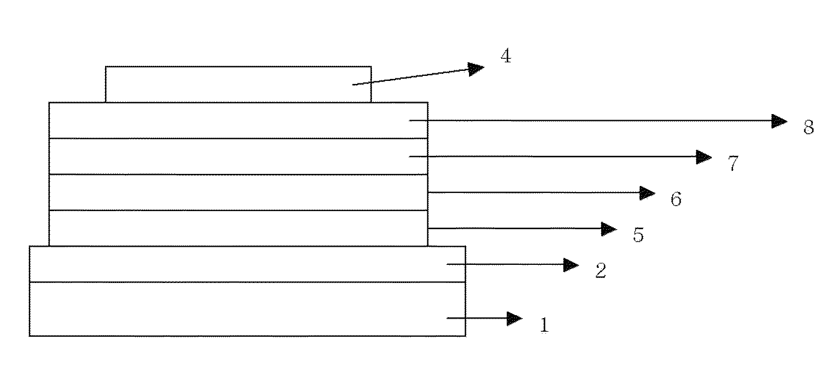
Image

Examples
example 1
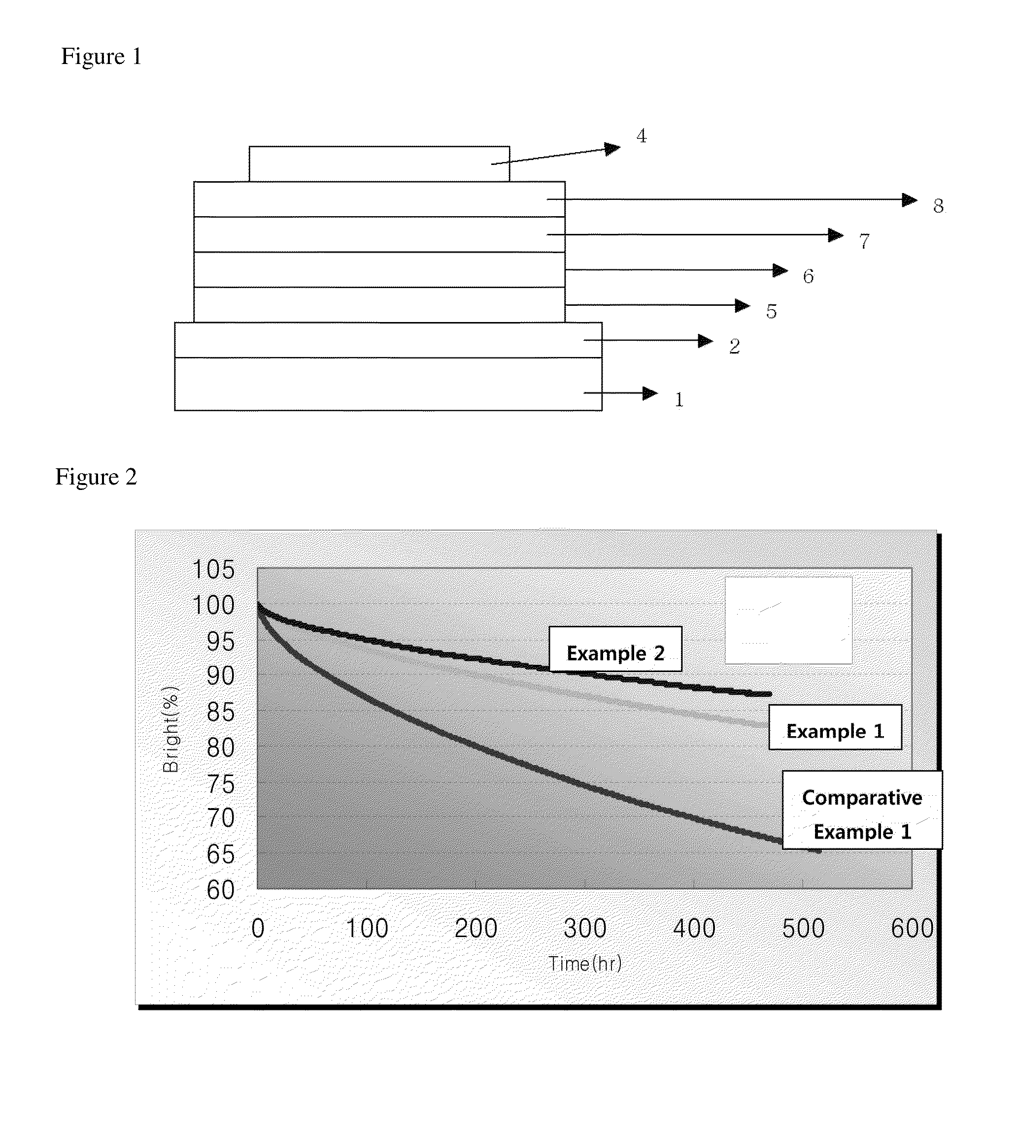
[0091]An organic light emitting diode was manufactured in the same manner as in Comparative Example 1, except that a compound of Formula 1-5 was deposited to a thickness of 40 nm instead of [cp2] as a hole transporting layer in Comparative Example 1.
example 2
[0092]An organic light emitting diode was manufactured in the same manner as in Example 1, except that a compound of Formula 1-5 and [cp3] were mixed at a ratio of 1:1 to form a film on the light emitting layer in Example 1.
example 3
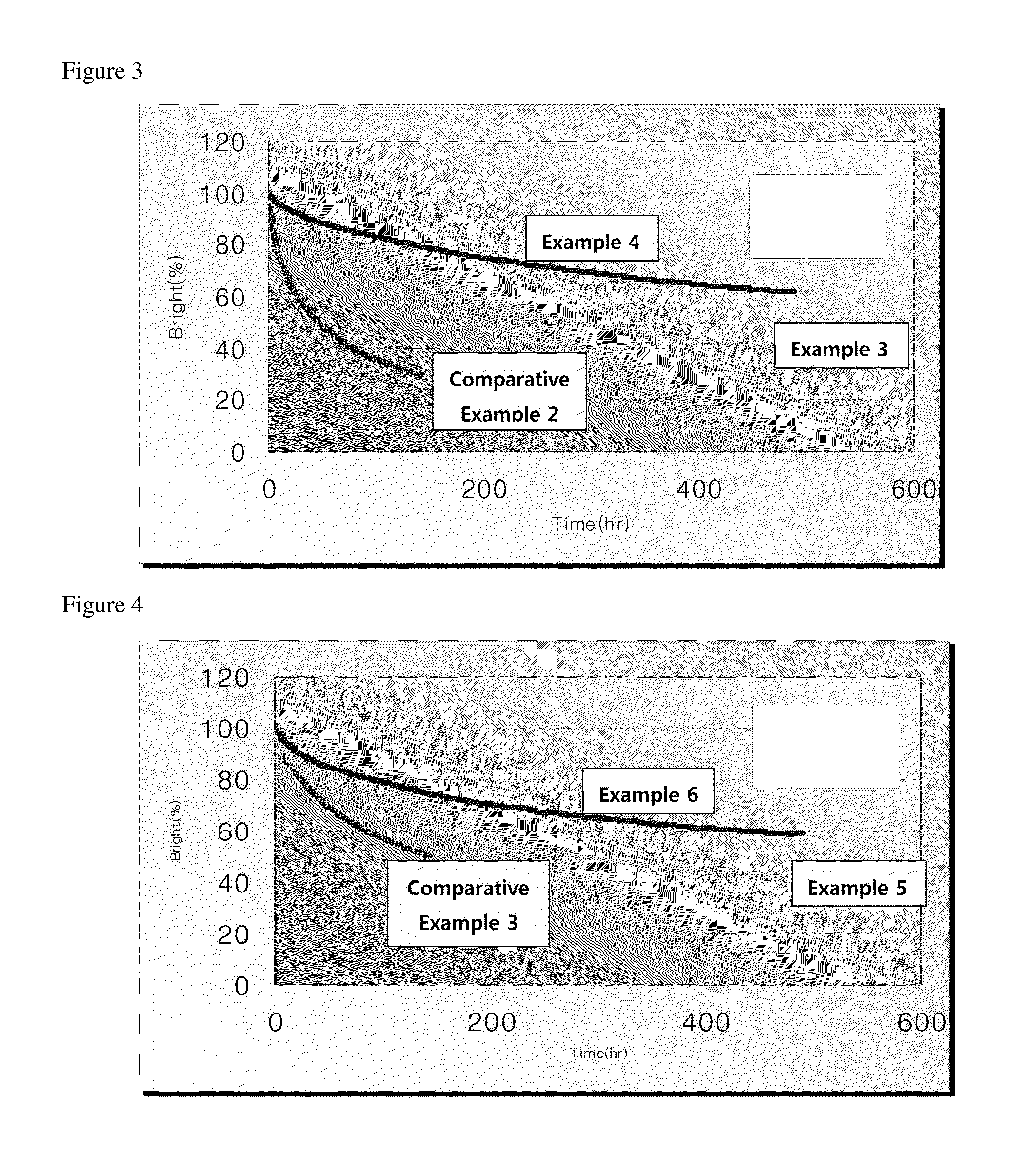
[0093]An organic light emitting diode was manufactured in the same manner as in Example 1, except that a compound of Formula [cp4] was deposited to a thickness of 40 nm instead of [cp3] as the light emitting layer in Example 1.
PUM
| Property | Measurement | Unit |
|---|---|---|
| internal quantum efficiency | aaaaa | aaaaa |
| current density | aaaaa | aaaaa |
| thickness | aaaaa | aaaaa |
Abstract
Description
Claims
Application Information
 - R&D
- Intellectual Property
- Life Sciences
- Materials
- Tech Scout
- Unparalleled Data Quality
- Higher Quality Content
- 60% Fewer Hallucinations
Browse by: Latest US Patents, China's latest patents, Technical Efficacy Thesaurus, Application Domain, Technology Topic, Popular Technical Reports.
© 2025 PatSnap. All rights reserved.Legal|Privacy policy|Modern Slavery Act Transparency Statement|Sitemap|About US| Contact US: help@patsnap.com