Optical sensor comprising a photodiode having a p-type semiconductor region, an intrinsic semiconductor region, and an n-type semiconductor region

a technology applied in the field of optical sensors and liquid crystal panels, can solve the problems of reducing light conversion efficiency, reducing light receiving area, and reducing output, so as to improve light detection sensitivity

Inactive Publication Date: 2014-09-30
SHARP KK
View PDF3 Cites 0 Cited by
  • Summary
  • Abstract
  • Description
  • Claims
  • Application Information

AI Technical Summary

Benefits of technology

[0007]It is an object of the present invention to provide an optical sensor having a novel structure with which, even if the substantial length of the intrinsic semiconductor region in the direction parallel with the forward direction of a photodiode is short, a sufficient light receiving area can be obtained, whereby the light detection sensitivity can be improved; and to provide a liquid crystal panel provided with the optical sensors.
[0009]With the optical sensor of the present invention, even if the intrinsic semiconductor region has a short substantial length in the direction parallel with the forward direction of the photodiode, a light receiving area can be ensured, whereby light detection sensitivity can be improved.

Problems solved by technology

Consequently, the other region than the region where the photoexcitation occurs in response to received light functions as a resistive region, thereby causing a decrease in the output.
On the other hand, if the intrinsic region has a too short length in the direction parallel with the forward direction of the photodiode, the region in which photoexcitation occurs in response to received light has a smaller area, thereby causing a decrease in the light conversion efficiency.
However, in the case of the photodiode described in Patent Document 1, if the distance between the two metal lines is shortened simply, this causes the light receiving area to decrease, which leads to a problem of difficulty in obtaining sufficient detection sensitivity.

Method used


Image

  • Optical sensor comprising a photodiode having a p-type semiconductor region, an intrinsic semiconductor region, and an n-type semiconductor region
  • Optical sensor comprising a photodiode having a p-type semiconductor region, an intrinsic semiconductor region, and an n-type semiconductor region
  • Optical sensor comprising a photodiode having a p-type semiconductor region, an intrinsic semiconductor region, and an n-type semiconductor region

Examples


embodiment 1

[Embodiment 1]

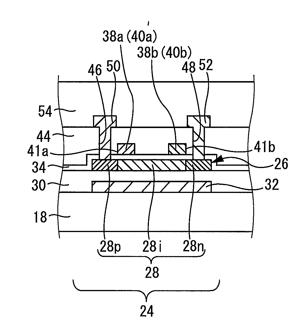
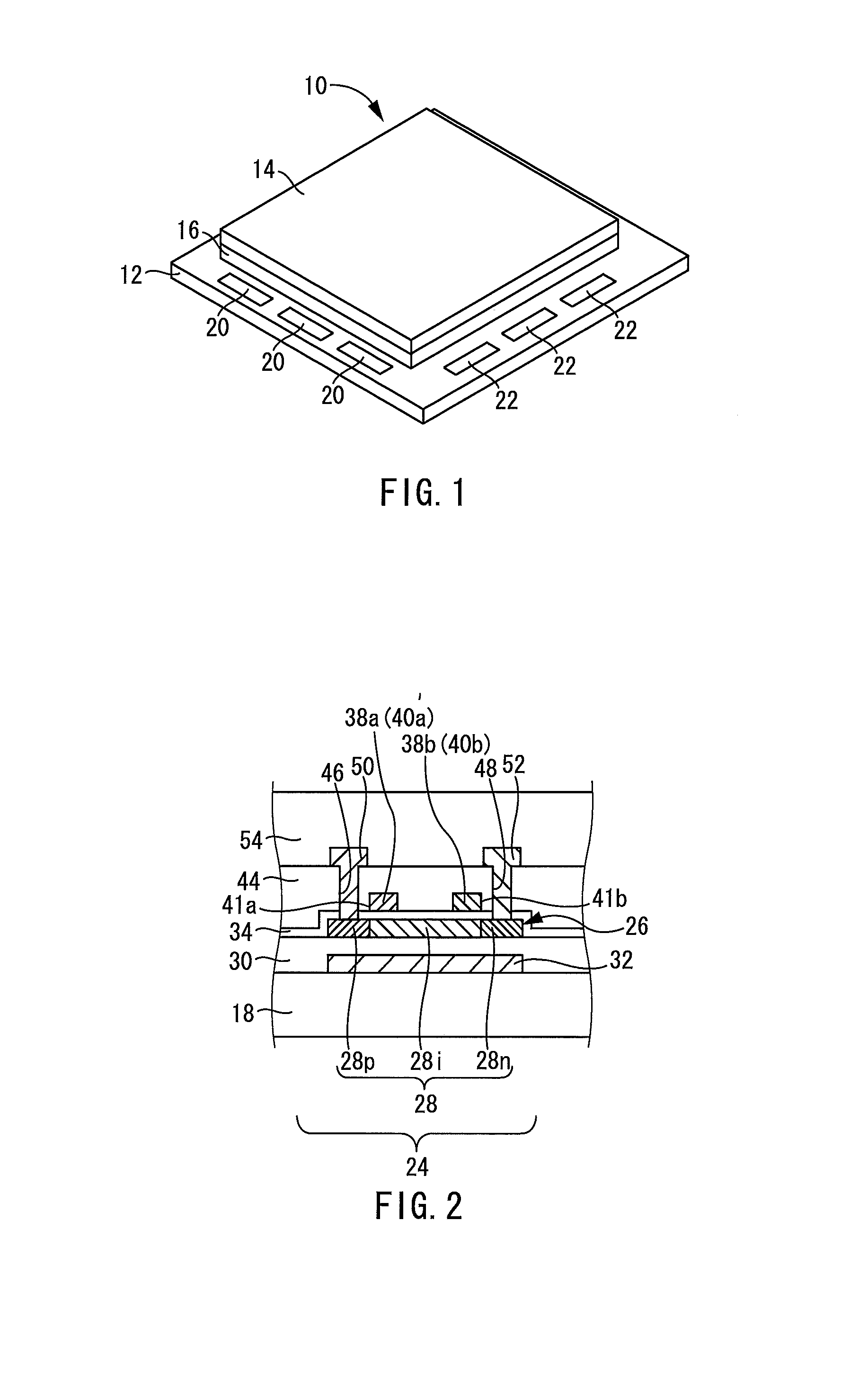
[0034]FIG. 1 shows a liquid crystal panel 10 as one embodiment of the present invention relating to a liquid crystal panel. This liquid crystal panel 10 includes an active matrix substrate 12, a counter substrate 14, and a liquid crystal layer 16 sealed between these substrates 12 and 14.

[0035]The active matrix substrate 12 includes a glass substrate 18 as a substrate (see FIG. 2). On the glass substrate 18, a plurality of pixels (not shown) are formed in matrix. Each pixel thus formed includes a thin film transistor as an active element, and a pixel electrode. On the glass substrate 18, a region where the plurality of pixels are formed in matrix is a display region, which is not shown.

[0036]At a position opposed to this display region, a counter substrate 14 is provided. It should be noted that a counter electrode and color filters are provided on the counter substrate 14, though not shown.

[0037]Further, on the glass substrate 18 provided in the active matrix substrat...

embodiment 2

[Embodiment 2]

[0088]Next, Embodiment 2 of the present invention relating to an optical sensor is explained based on FIG. 5. It should be noted that members and portions in Embodiment 2 described below, and in Embodiment 3 to be described later, having the same configurations as those in Embodiment 1, are denoted by the same reference numerals as those in Embodiment 1 in the drawings, and detailed explanations of the same are omitted.

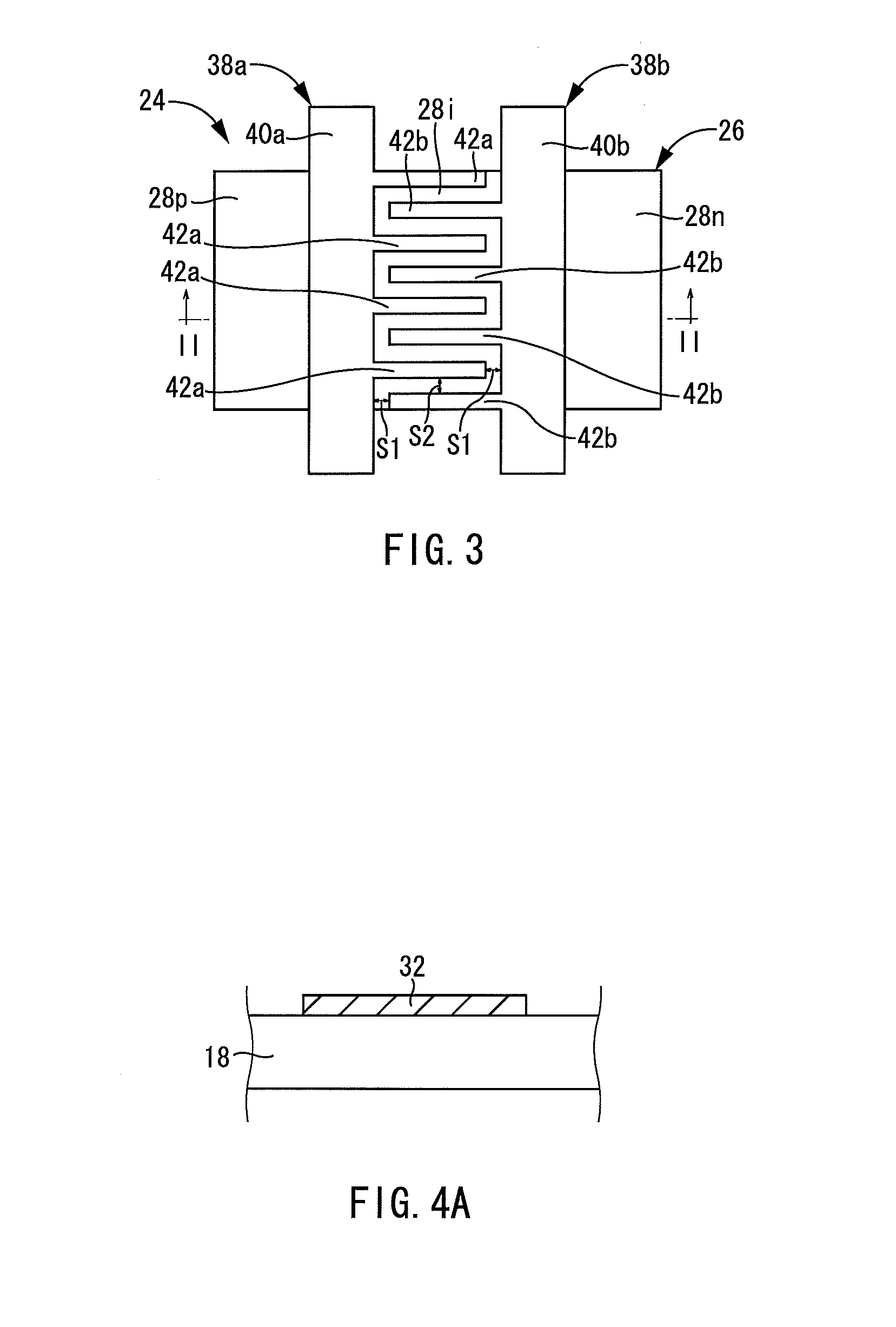
[0089]An optical sensor 64 of the present embodiment is different from the optical sensor (24) of Embodiment 1 regarding extension lines 66a and 66b in the gate lines 38a and 38b. The extension lines 66a and 66b of the present embodiment include parallel extension portions 68a and 68b, and perpendicular extension portions 70a and 70b, respectively.

[0090]The parallel extension portions 68a and 68b extend in the direction parallel with the forward direction of the photodiode 26, with approximately constant line widths, from the boundary definition lines 40...

embodiment 3

[Embodiment 3]

[0092]Next, Embodiment 3 of the present invention relating to an optical sensor is explained based on FIG. 6. An optical sensor 72 of the present embodiment is different from the optical sensor (24) of Embodiment 1 regarding extension lines 74a and 74b of the gate lines 38a and 38b.

[0093]The extension lines 74a and 74b of the present embodiment are shaped so that a line width of each decreases with increasing proximity to the end in the extending direction. Clearances S6 formed between extension ends of the extending lines 74a and 74b and the boundary definition lines 40b and 40a, respectively, and a clearances S7 formed between the extension line 74a and the extension line 74b may have a width of 3 to 5 μm each.

[0094]The embodiments of the present invention, which have been described in detail so far, are merely illustrative examples, and the present invention is not limited by the above-described embodiments at all.

[0095]For example, in Embodiments 1 to 3, the appli...


PUM

PropertyMeasurementUnit
widthaaaaaaaaaa
thicknessaaaaaaaaaa
thicknessaaaaaaaaaa

Abstract

Provided is an optical sensor having such a novel structure that even if an intrinsic semiconductor region has a short substantial length in a direction parallel with a forward direction of a photodiode, a light receiving area can be ensured, whereby light detection sensitivity can be improved; and a liquid crystal panel including the optical sensor. The optical sensor includes: a photodiode (26) provided with a semiconductor film (28) having a p-type semiconductor region (28p), an intrinsic semiconductor region (28i), and an n-type semiconductor region (28n); a first gate line (38a) formed above the intrinsic semiconductor region (28i), a negative voltage being applied to the first gate line; and a second gate line (38b) formed above the intrinsic semiconductor region (28i), a positive voltage being applied to the second gate line, wherein a predetermined clearance is formed between the first gate line (38a) and the second gate line (38b), above the intrinsic semiconductor region (28i).

Description

TECHNICAL FIELD[0001]The present invention relates to an optical sensor, and a liquid crystal panel provided with the optical sensor.BACKGROUND ART[0002]Conventionally, a liquid crystal display device provided with optical sensors has been known, as a device that realizes a touch sensor function and the like. In such a liquid crystal display device, from the viewpoint of the reduction of the number of components, and the like, optical sensors are formed monolithically in an active matrix substrate incorporated in a liquid crystal panel. A well-known example of such an optical sensor is a photodiode having a lateral structure.[0003]In the photodiode having the lateral structure, if the intrinsic semiconductor region has a too large length in the direction parallel with the forward direction of the photodiode, a region in which photoexcitation occurs in response to received light does not extent over an entirety of the intrinsic semiconductor region. Consequently, the other region tha...

Claims


Application Information

Patent Timeline
Patent Type & Authority Patents(United States)
IPC IPC(8): G02F1/136H01L27/15G02F1/133H01L27/148G02F1/1333G02F1/135H01L27/146H01L31/0224H01L31/105H01L31/113
CPCH01L27/14643H01L31/1055H01L31/022408G02F1/13338H01L31/1133H01L31/105G02F1/1354
Inventor TAKAIWA, NORIHISAFUJIWARA, MASAHIRO
Owner SHARP KK
Why Eureka
Try Eureka