Process for producing indium oxide-containing layers

a technology of indium oxide and containing layers, which is applied in the direction of liquid/solution decomposition chemical coatings, coatings, electrical devices, etc., can solve the problems of reduced quality of halogen-containing layers, inability to produce fine structures, and high cost and inconvenience of the process described in the documen

Active Publication Date: 2014-10-14
EVONIK OPERATIONS GMBH
View PDF19 Cites 5 Cited by
  • Summary
  • Abstract
  • Description
  • Claims
  • Application Information

AI Technical Summary

Problems solved by technology

Moreover, it was hitherto assumed that halogen-containing precursors potentially had the disadvantage of leading to halogen-containing layers of reduced quality.
The processes described therein, however, are very costly and inconvenient, and / or are based on reactants which are not available commercially (and must therefore, as a disadvantage, be synthesized in a step beforehand).
Conversion carried out by means of heat alone, however, has the disadvantage that it cannot be used to produce fine structures and that, furthermore, it does not allow precise control over the resulting layer properties.
Conversions which take place exclusively by radiation, however, have the disadvantage that they require very high energy densities over a relatively long time and are therefore very costly and inconvenient in terms of apparatus.
The known processes for producing indium oxide-containing layers via combined thermal conversion and conversion with electromagnetic radiation, however, have the disadvantage that the use of the indium alkoxides described exhaustively in the literature exhibits much poorer semiconducting properties.
Furthermore, even the combination of thermal conversion with conversion by means of electromagnetic or UV radiation alone does not result in sufficiently satisfactory results, particularly in relation to the resultant field-effect mobilities μFET.
The problem posed, therefore, is that of overcoming the outlined disadvantages of the prior art and of providing an improved process for producing indium oxide-containing layers.

Method used


Image

  • Process for producing indium oxide-containing layers
  • Process for producing indium oxide-containing layers

Examples


examples

Inventive Example

Indium Chlorine Alkoxide as Precursor

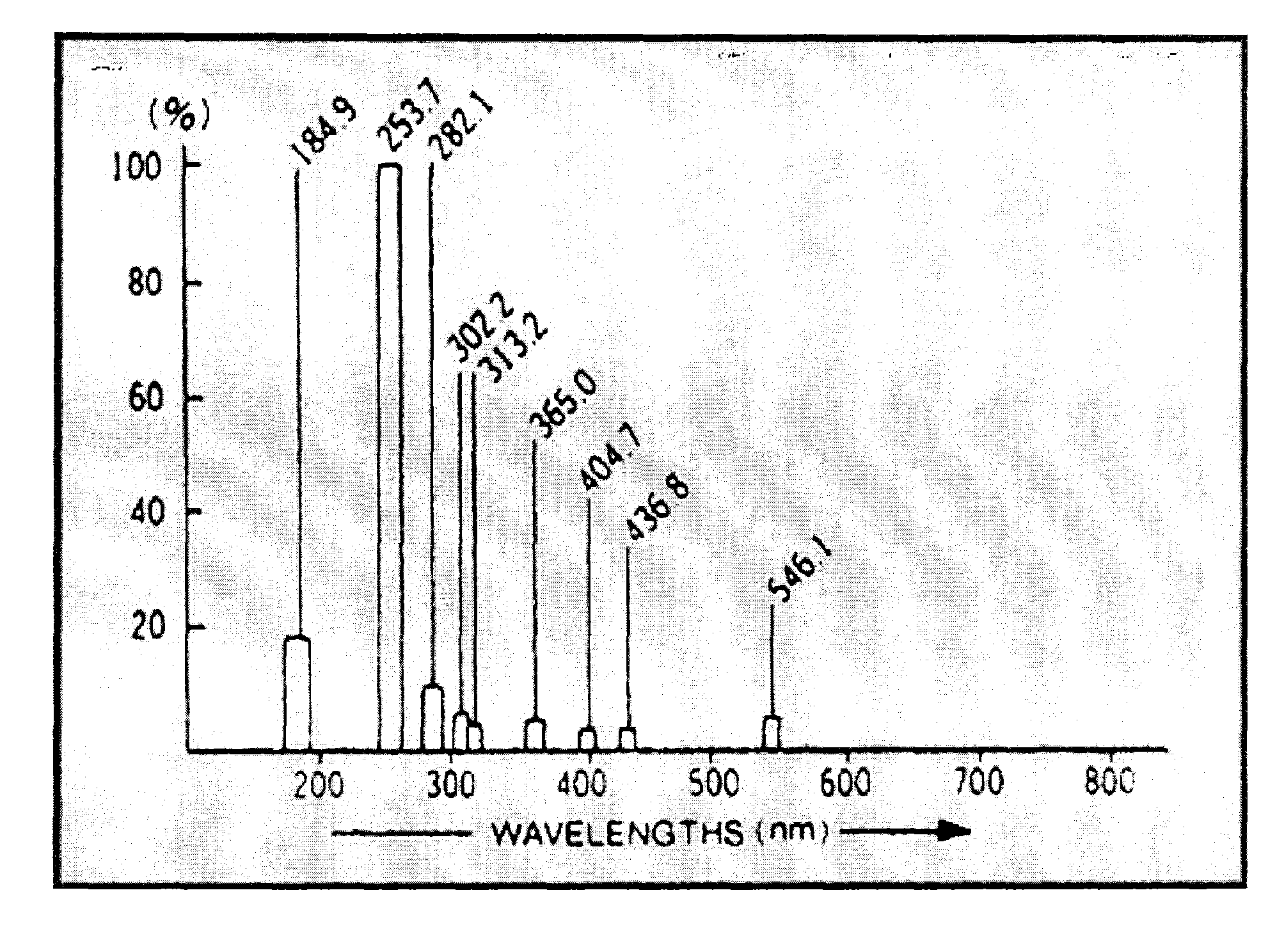
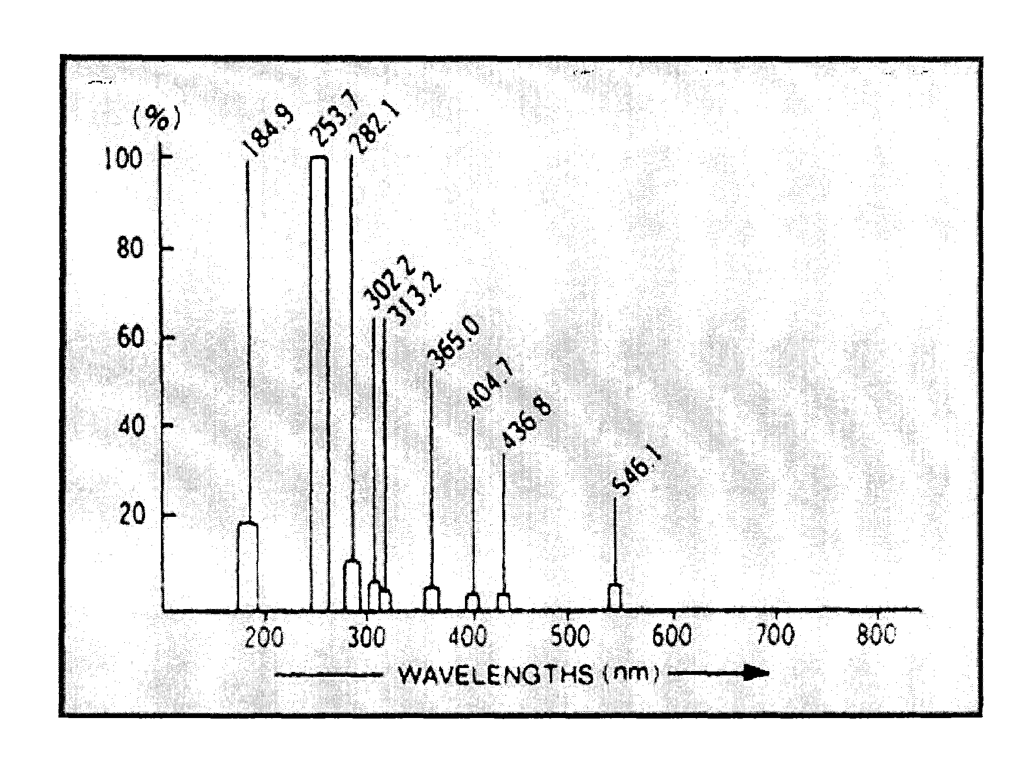
[0080]100 μl of a 1.0% by weight solution of InCl(OMe)2 in ethanol were applied to a doped silicon substrate having an edge length of approximately 15 mm, with a silicon oxide coating around 200 nm thick and with finger patterns made of ITO / gold. This is followed by spin coating at 2000 rpm (5 seconds). Directly after this coating procedure, the coated substrate is irradiated for 5 minutes with UV radiation from a mercury vapour lamp (illuminant GLF-100, Jelight 144AX-220, quartz glass, Jelight) in the wavelength range of 150-300 nm. The substrate is then heated for an hour on a hotplate at a temperature of 350° C. Following conversion, a field-effect mobility μFET value of 8.5 cm2 / Vs can be determined in a glove box.

Comparative Example

Indium Alkoxide as Precursor

[0081]100 μl of a 1.0% by weight solution of In(OiPr)3 in ethanol were applied to a doped silicon substrate having an edge length of approximately 15 mm, with a silicon ...


PUM

PropertyMeasurementUnit
temperatureaaaaaaaaaa
source-drain voltageaaaaaaaaaa

Abstract

The present invention relates to a liquid phase process for producing indium oxide-containing layers, in which a coating composition preparable from a mixture comprising at least one indium oxide precursor and at least one solvent and / or dispersion medium, in the sequence of points a) to d), a) is applied to a substrate, and b) the composition applied to the substrate is irradiated with electromagnetic radiation, c) optionally dried and d) converted thermally into an indium oxide-containing layer, where the indium oxide precursor is an indium halogen alkoxide of the generic formula InX(OR)2 where R is an alkyl radical and / or alkoxyalkyl radical and X is F, Cl, Br or I and the irradiation is carried out with electromagnetic radiation having significant fractions of radiation in the range of 170-210 nm and of 250-258 nm, to the indium oxide-containing layers producible with the process, and the use thereof.

Description

FIELD OF THE INVENTION[0001]The present invention relates to a process for producing indium oxide-containing layers, to the indium oxide-containing layers producible with the process of the invention, and to the use thereof.[0002]The production of semiconducting electronic component layers by means of printing and other liquid deposition processes enables a simplification in terms of process technology and much lower production costs compared to many other processes, for example chemical vapour deposition (CVD), since the semiconductor can be deposited here in a continuous operation. Furthermore, in the case of lower operational temperatures, it becomes possible to work on flexible substrates as well, and optionally (especially in the case of very thin layers and more particularly with oxidic semiconductors) to achieve optical transparency in the printed layers. Semiconducting layers, here and below, are layers which have charge carrier mobilities of 1 to 50 cm2 / Vs for a component w...

Claims


Application Information

Patent Timeline
Patent Type & Authority Patents(United States)
IPC IPC(8): H01L21/16H01L29/10B05D5/12H01L21/12C23C18/12H01L21/02H01L21/288H01L29/22H01L29/43
CPCH01L21/02628H01L21/288H01L29/22C23C18/1216H01L29/43C23C18/12C23C18/18
Inventor STEIGER, JUERGENPHAM, DUY VUTHIEM, HEIKOMERKULOV, ALEXEYHOPPE, ARNE
Owner EVONIK OPERATIONS GMBH
Why Eureka
Try Eureka