Arrangements and methods for determining positions and offsets

a technology of position and offset, applied in the direction of instruments, coatings, measurement devices, etc., can solve the problems of affecting the processing efficiency of wafers, the inability to accurately align the end effector center, and the rare event of ideal scenario

Active Publication Date: 2014-10-14
LAM RES CORP
View PDF54 Cites 280 Cited by
  • Summary
  • Abstract
  • Description
  • Claims
  • Application Information

AI Technical Summary

Problems solved by technology

However, for many reasons, some of which are discussed below, this ideal scenario is rarely the case.
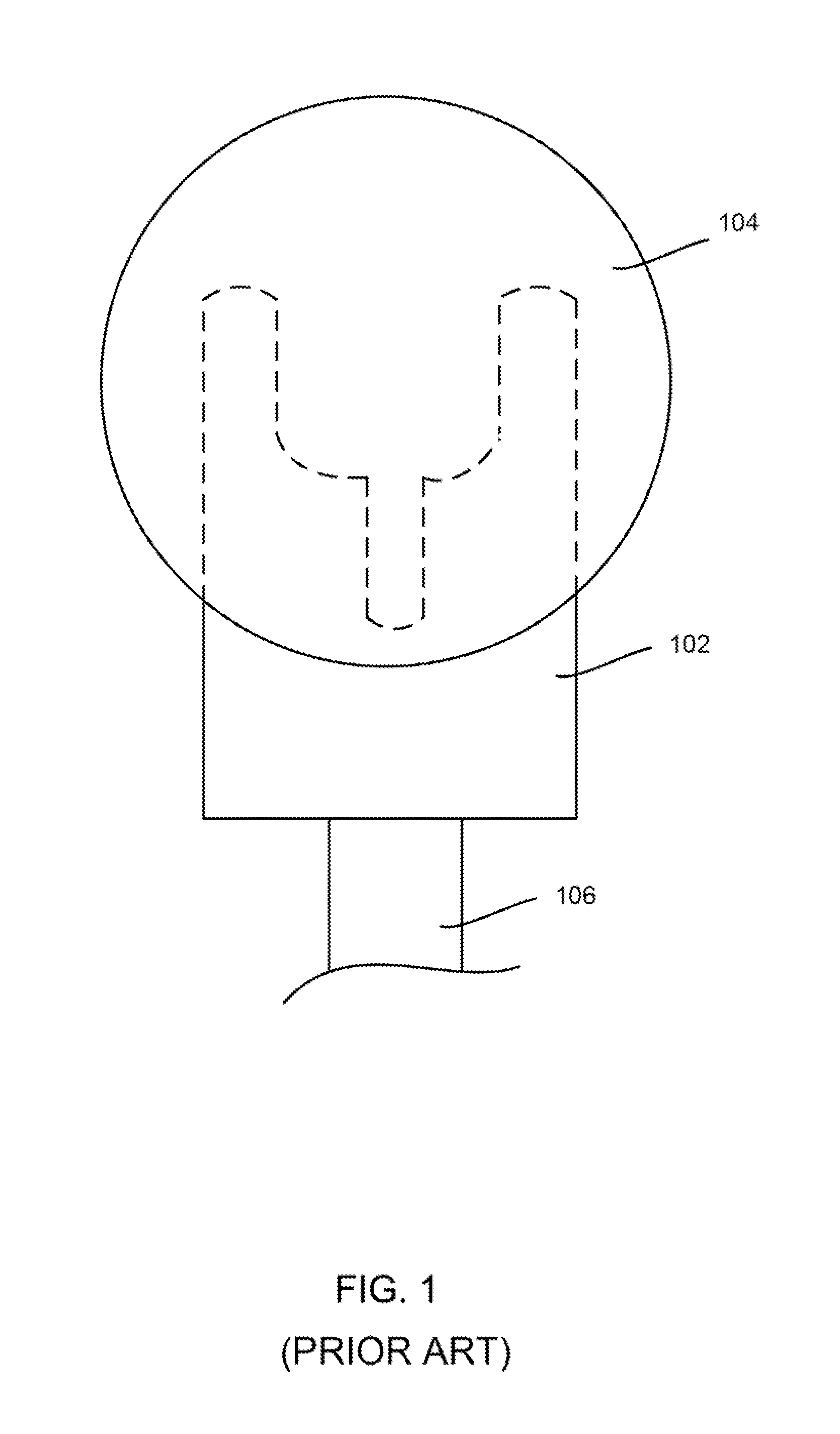
As a result, it is possible that the end effector-defined center may not be correctly aligned with the center of the chuck at the robot arm position that the robot controller deems to be the correct position for wafer placement.
If this end effector / chuck mis-alignment is not compensated for during production, the wafer may be inaccurately placed relative to the chuck center during wafer processing.
However, there are disadvantages with the prior art technique for centering the end effector relative to the chuck for calibration purposes.
Also, affixing a physical mechanical fixture, which may have one or more hard metal edges or surfaces, on the chuck may potentially damage the chuck.
Additionally, if this calibration is done in the field after some plasma cycles have been executed in the processing module (e.g., in response to a concern that the end effector may not be centered relative to the chuck following a production run), the attachment of a physical calibration fixture on the chuck may cause deposited particles on or near the chuck to flake off into the processing chamber.
During the subsequent processing cycles, such particles constitute particle contamination, which is undesirable.
Additionally, because the calibration is performed at atmospheric pressure, the prior art calibration technique may not effectively duplicate the conditions that exist during production.
Since the calibration conditions do not faithfully duplicate the production conditions, accurate calibration may not be possible.
When the robot arm pulls away, even by a small amount that may be imperceptible to the robot operator, this shift may result in inaccuracy in the calibration process.
If the calibration process is inaccurate, inaccurate wafer placement during production may occur, leading to decreased yield and an increase in the rejection and / or failure rate for the fabricated products.
However, even if the end effector-defined center is correctly aligned with the chuck center (or can be made to achieve the effect of a correct alignment), there exists another potential source of error that may result in wafer / chuck mis-alignment during production.
If the end effector-defined center is not correctly or consistently aligned with the center of the wafers, wafer / chuck mis-alignment may still occur during production.
The same manufacturing and assembly tolerance issues also affect the alignment of the upper electrode relative to the lower electrode.
For example, in some production plasma processing systems, manufacturing and assembly tolerances may cause the upper electrode to be slightly offset from the chuck, resulting in an asymmetrical plasma sheath, which affects the controllability of the plasma processing.
Over time, the upper electrode assembly may develop “play” or out-of-spec tolerances, resulting in a detrimental upper electrode / chuck offset.
As a result, plasma processing result may suffer.
As can be seen from the foregoing, various misalignment issues may exist and / or develop over time between components in a plasma processing module.
As discussed, if these misalignment issues are addressed using external tools or external alignment fixtures, potential damage to the processing module components may result.
Further, if the misalignment issues are addressed outside of the processing module environment, errors may arise due to the dissimilarities in chamber conditions (e.g., the dissimilarities in chamber conditions that exist during alignment and chamber conditions that exist during production).
Still further, if the prior art requires shuffling wafers in and out of the processing module in order to address misalignment issues, an undue amount of time may be wasted on alignment issues alone.
The wasted time contributes to a higher cost of ownership for operators of plasma processing tools, which tends to translate into lower production of finished devices per unit of time and / or higher per-unit device cost.

Method used


Image

  • Arrangements and methods for determining positions and offsets
  • Arrangements and methods for determining positions and offsets
  • Arrangements and methods for determining positions and offsets

Examples


Embodiment Construction

[0027]The present invention will now be described in detail with reference to a few embodiments thereof as illustrated in the accompanying drawings. In the following description, numerous specific details are set forth in order to provide a thorough understanding of the present invention. It will be apparent, however, to one skilled in the art, that the present invention may be practiced without some or all of these specific details. In other instances, well known process steps and / or structures have not been described in detail in order to not unnecessarily obscure the present invention.

[0028]Various embodiments are described herein below, including methods and techniques. It should be kept in mind that the invention might also cover articles of manufacture that includes a computer readable medium on which computer-readable instructions for carrying out embodiments of the inventive technique are stored. The computer readable medium may include, for example, semiconductor, magnetic,...


PUM

PropertyMeasurementUnit
reflectivityaaaaaaaaaa
hardaaaaaaaaaa
atmospheric pressureaaaaaaaaaa

Abstract

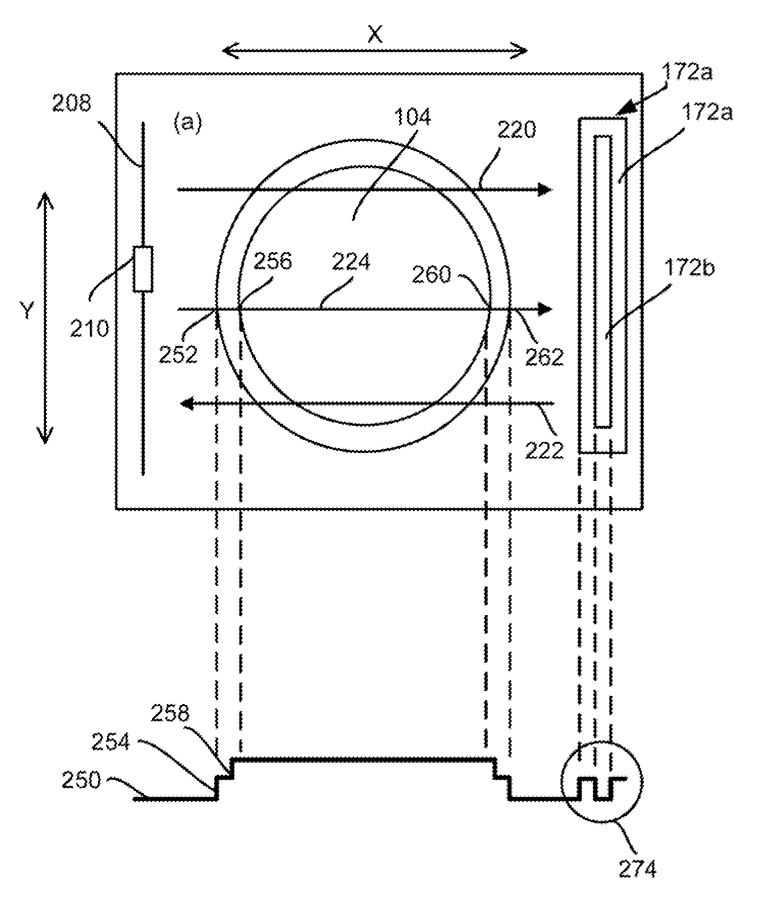
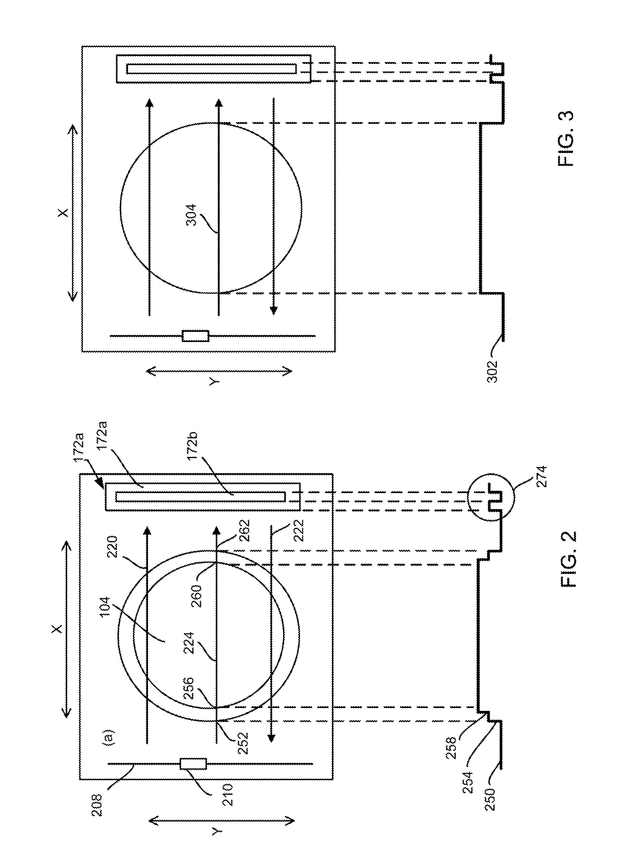
A method for determining positions and offsets in a plasma processing system, the plasma processing system including at least a chuck and an upper electrode is provided. The method including moving a traversing assembly along a first plurality of paths to generate a first plurality of data sets, the traversing assembly including at least a light source, the light source providing a light beam, moving the traversing assembly along each path of the first plurality of paths causing the light beam to traverse the chuck and resulting in one or more data sets of the first plurality of data sets. The method also including receiving the first plurality of data sets and analyzing the first plurality of data sets to identify a first set of at least three discontinuities, wherein the first set of at least three discontinuities are related to three or more reflected light signals generated when the light beam encounters an edge of the chuck. The method also including determining a center of the chuck using coordinate data associated with the first set of at least three discontinuities.

Description

PRIORITY CLAIM[0001]This application is related to and claims priority under 35 U.S.C. §119(e) to a commonly assigned provisional patent application entitled “In-Situ Optical Techniques for Determining Positions and Offsets,” by Allen-Blanchette et al., Application Ser. No. 61 / 017,148, filed on Dec. 27, 2007, and under 35 U.S.C. 371 to a PCT Application No. PCT / US2008 / 087578, filed on Dec. 19, 2008, all of which are incorporated herein by reference.BACKGROUND OF THE INVENTION[0002]In the processing of semiconductor substrates (e.g., wafers), plasma is often employed. In plasma processing, the wafers are processed using a plasma processing system, which typically includes a plurality of processing modules. The substrate (e.g., wafer) is disposed on a chuck inside a processing module during plasma processing.[0003]In order to move a wafer in and out of the processing module, the wafer is typically placed on an end effector and transferred onto the chuck. The end effector is a structur...

Claims


Application Information

Patent Timeline
Patent Type & Authority Patents(United States)
IPC IPC(8): G01B11/14G01B11/27H01L21/67
CPCH01L21/67069G01B11/272G01B11/14H01L21/67265
Inventor RODNICK, MATTALLEN-BLANCHETTE, CHRISTINE
Owner LAM RES CORP
Why Eureka
Try Eureka