Heterojunction bipolar transistor manufacturing method and integrated circuit comprising a heterojunction bipolar transistor

a manufacturing method and heterojunction technology, applied in the direction of basic electric elements, electrical apparatus, semiconductor devices, etc., can solve the problems the performance limitation factor of the hbt in the baseline cmos process, and the inability to meet the requirements of the hbt, so as to reduce the collector resistance and increase the complexity of the manufacturing process. , the effect of increasing the complexity of the manufacturing process

Active Publication Date: 2014-10-28
NXP BV
View PDF16 Cites 2 Cited by
  • Summary
  • Abstract
  • Description
  • Claims
  • Application Information

AI Technical Summary

Benefits of technology

[0018]The present invention seeks to provide a method of manufacturing a HBT in which the collector resistance may be reduced without reducing the open-base breakdown voltage of the HBT and / or without increasing the complexity of the manufacturing process.
[0019]The present invention further seeks to provide a HBT having a reduced collector resistance and an improved open-base breakdown voltage.

Problems solved by technology

This is not trivial, at least from a cost perspective, as the most advanced CMOS nodes in currently in production are too expensive for e.g. the component business and RF / AMS stand-alone products.
A performance-limiting factor in a HBT in a baseline CMOS process is the intrinsic resistance of the connection between the collector contact (plug) and the buried or implanted active collector region of the HBT device.
Firstly, the collector contact resistance may be too high, which results in low DC / RF performance. For performance in the 50 GHz range, the collector resistance is important but not limiting. However, as the base and collector profiles are optimized for higher fT, collector resistance becomes increasingly critical. Therefore, the tradeoffs with respect to reducing the collector resistance while minimizing process complexity become more significant and challenging. As an example, FIG. 1 demonstrates a 1D TCAD simulation of peak-fT versus total collector resistance. The 1D simulation was performed for a doping profile that is representative for an implanted collector that contains a selectively implanted collector (SIC) used to locally increase the collector dope and obtain higher RF performance).
Despite the decrease in sinker resistance and increase of RF performance for optimal sinker implant conditions, one drawback of the standard approach is the need for an extra sinker mask, which adds to the cost and complexity of the manufacturing process.
Secondly, the collector sinker can have a negative impact on the device breakdown characteristics.
From these results it is clear that high collector sinker dope to reduce the collector resistance, thereby improving RF performance and reducing noise as discussed previously has the disadvantage of higher active region dope due to sinker diffusion.
Therefore, high sinker doping levels for low resistive path and high RF performance are not always compatible with “high” breakdown voltage and minimum device area.

Method used


Image

  • Heterojunction bipolar transistor manufacturing method and integrated circuit comprising a heterojunction bipolar transistor
  • Heterojunction bipolar transistor manufacturing method and integrated circuit comprising a heterojunction bipolar transistor
  • Heterojunction bipolar transistor manufacturing method and integrated circuit comprising a heterojunction bipolar transistor

Examples


Embodiment Construction

[0030]Embodiments of the invention are described in more detail and by way of non-limiting examples with reference to the accompanying drawings, wherein:

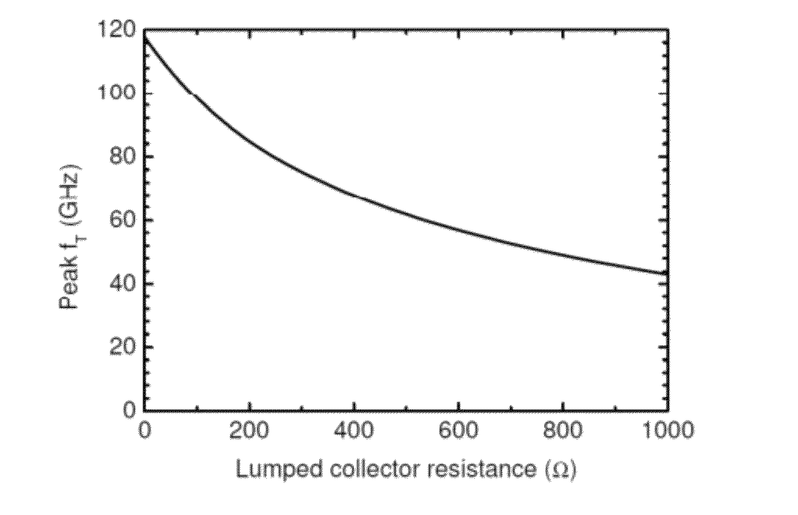
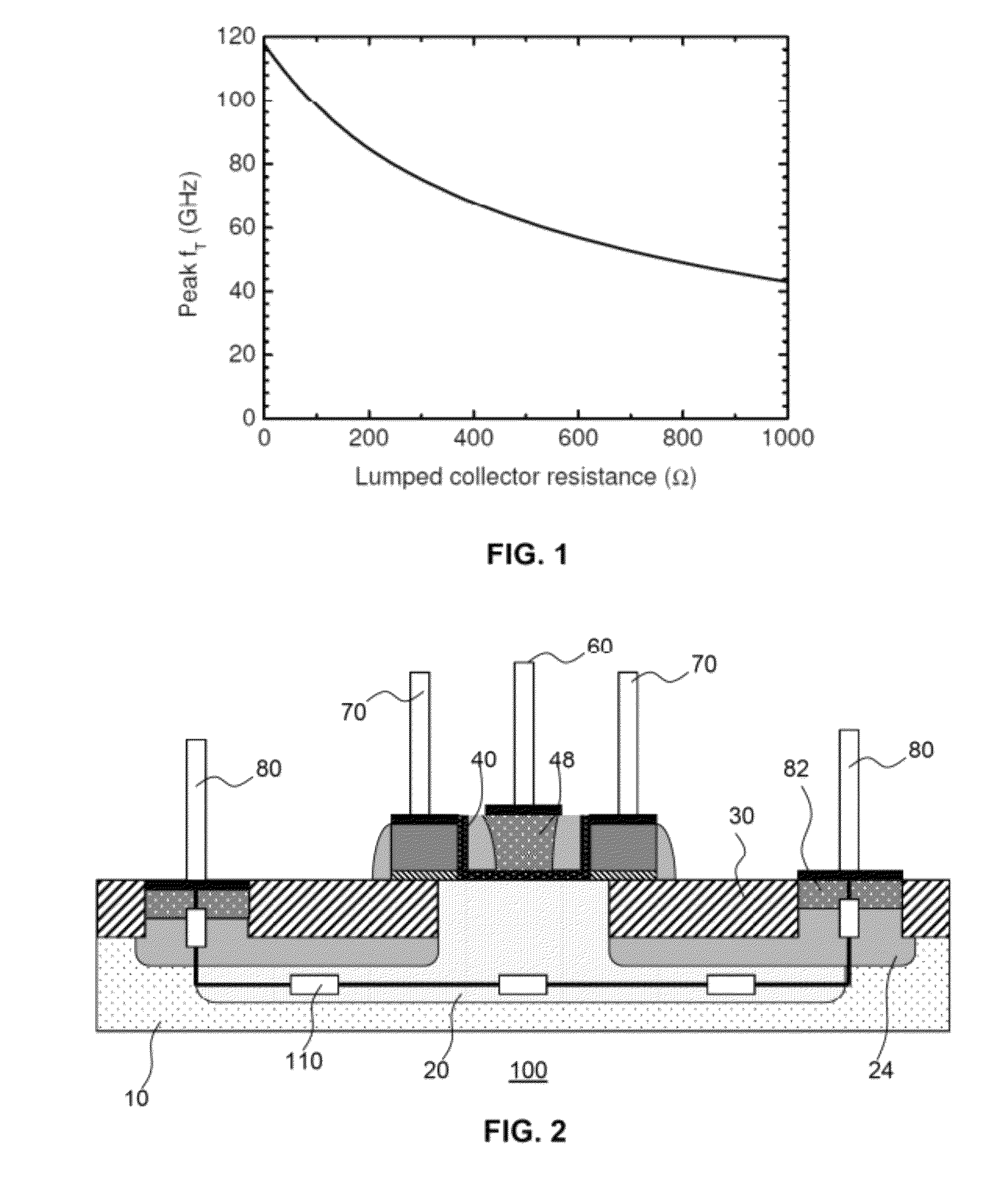
[0031]FIG. 1 depicts the result of a 1D TCAD simulation of peak-fT versus total collector resistance of a HBT;

[0032]FIG. 2 schematically depicts a prior art HBT;

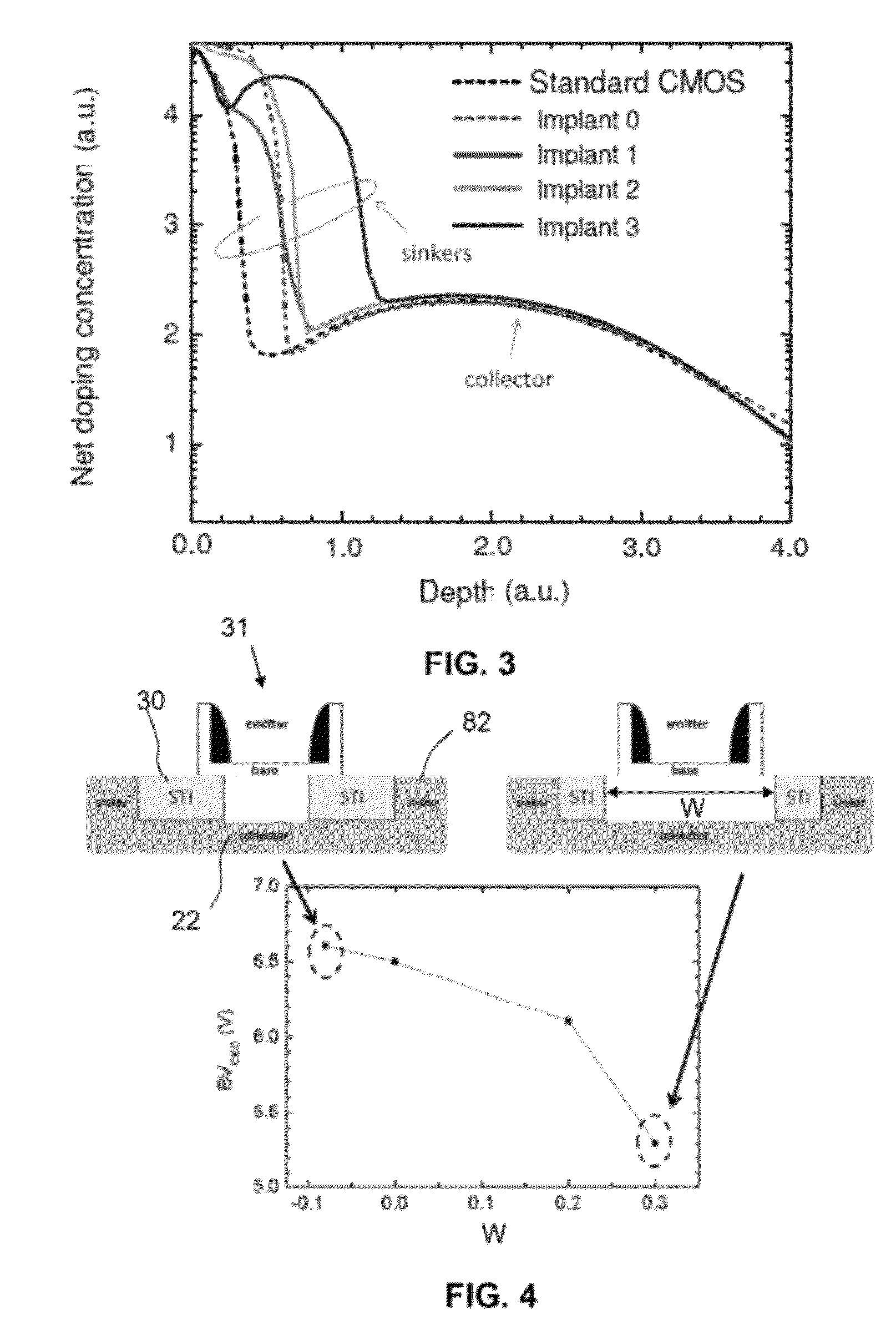
[0033]FIG. 3 schematically depicts a number of doping profiles for a collector sinker plug of a HBT;

[0034]FIG. 4 schematically depicts the effect of active region width variation on the breakdown voltage of a HBT;

[0035]FIG. 5a-p schematically depicts the steps of a method of manufacturing a HBT in accordance with an embodiment of the present invention;

[0036]FIG. 6 schematically depicts a HBT obtained with a variation to the method schematically depicted in FIG. 5a-p;

[0037]FIG. 7a-j schematically depicts the steps of a method of manufacturing a HBT in accordance with another embodiment of the present invention; and

[0038]FIG. 8a-i schematically depicts the steps of a method o...


PUM


Abstract

Disclosed is a method of manufacturing a heterojunction bipolar transistor comprising a substrate, an upper region of said substrate comprising an active region of the bipolar transistor bordered by shallow trench insulation, said active region comprising a buried collector region extending to a depth beyond the depth of the shallow trench insulation, the method comprising forming a trench in the substrate adjacent to said active region, said trench extending through the shallow trench insulation; at least partially filling said trench with an impurity; and forming a collector sinker in the substrate by developing said impurity to extend into the substrate to a depth beyond the depth of the shallow trench insulation. An IC comprising a heterojunction bipolar transistor manufactured by this method is also disclosed.

Description

[0001]This application claims the priority under 35 U.S.C. §119 of European patent application no. 10192804.2, filed on Nov. 26, 2010, the contents of which are incorporated by reference herein.FIELD OF THE INVENTION[0002]The present invention relates to a method of manufacturing a heterojunction bipolar transistor comprising a substrate, an upper region of said substrate comprising an active region of the bipolar transistor bordered by shallow trench insulation, said active region comprising a buried collector region extending to a depth beyond the depth of the shallow trench insulation.[0003]The present invention further relates to an integrated circuit comprising a heterojunction bipolar transistor comprising a substrate, an upper region of said substrate comprising an active region of the bipolar transistor bordered by shallow trench insulation, said active region comprising a buried collector region extending to a depth beyond the depth of the shallow trench insulation.BACKGROU...

Claims


Application Information

Patent Timeline
Patent Type & Authority Patents(United States)
IPC IPC(8): H01L29/08H01L29/737H01L29/66
CPCH01L29/0821H01L29/7378H01L29/66242
Inventor VANHOUCKE, TONYDONKERS, JOHANNES JOSEPHUS THEODORUS MARINUSMERTENS, HANSDURIEZ, BLANDINEGRIDELET, EVELYNE
Owner NXP BV
Why Eureka
Try Eureka