Trench power MOSFET structure and fabrication method thereof

a technology of power mosfet and fabrication method, which is applied in the direction of basic electric elements, electrical apparatus, and semiconductor devices, can solve the problems of not being able to manufacture power mosfets with better voltages withstanding capability and low impedance characteristics, and achieves reduced surface electric filed effect, less space, and less conduction loss (ron).

Active Publication Date: 2014-10-28
SUPER GROUP SEMICON
View PDF4 Cites 9 Cited by
  • Summary
  • Abstract
  • Description
  • Claims
  • Application Information

AI Technical Summary

Benefits of technology

[0018]To sum up, an exemplary embodiment of the present disclosure provides a trench power MOSFET structure and fabrication method thereof. In which repeat to fabricate the junction profile outward around the trench. Through controlling the amount of the implanted ions changes the width of the junction profile in design need. As the MOSFET is operated in reversed voltage, the electric potential is utilized to form the charge balance and reduced surface electric filed effect (RESURF). Accordingly, the moderate electric filed would be formed in the trench and the side surface of the trench. Consequently, utilize less space to obtain the property of the higher electric potential integration and less conduction loss (RON). Meanwhile, through the principle optimize the impedance and thickness of the epitaxial layer to decrease the conduction loss effectively and further reduce the conduction loss of the device.

Problems solved by technology

In the traditional fabrication method, the junction profile could not be controlled and therefore it could not to manufacture the power MOSFET with better voltages withstanding capability and low impedance characteristics.

Method used


Image

  • Trench power MOSFET structure and fabrication method thereof
  • Trench power MOSFET structure and fabrication method thereof
  • Trench power MOSFET structure and fabrication method thereof

Examples


Embodiment Construction

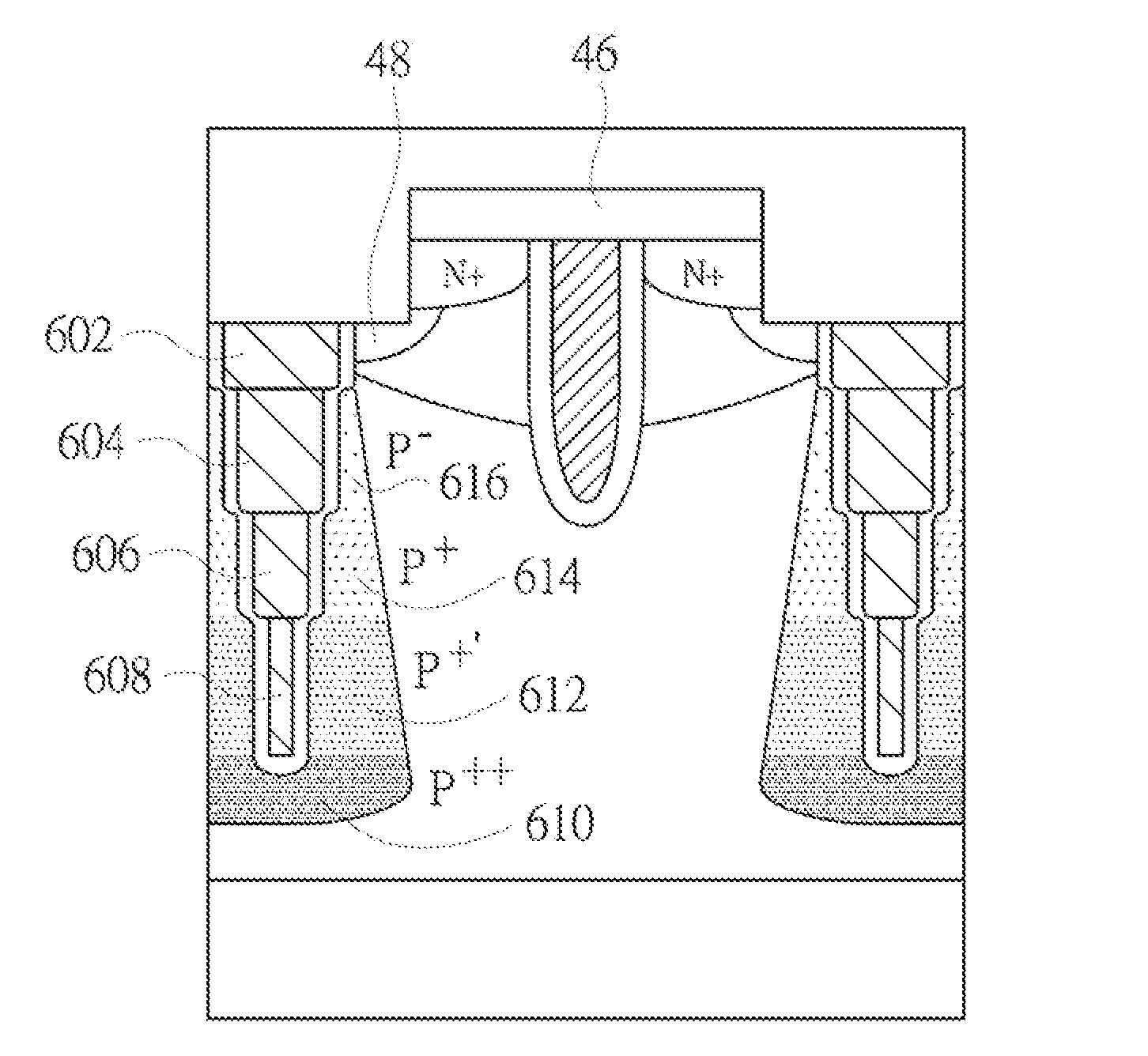
[0027]The main technique characteristic of present disclosure is to manufacture repeatedly at least two doped regions connecting to each other for forming the junction profile around the side wall of the trench. The junction profile can be controlled by the mounts of the ion implantations (dopant concentration) and the width of the junction profile is also defined. It can form the moderate electric field distribution in the trench and around the side wall of the trench to reduce effectively the conduction loss of the device. The design of the present disclosure can be applied to the trenches in the active region or termination region by controlling the dopant concentrations to form the junction profiles for achieving efficiently voltage withstanding capability and low impedance characteristics.

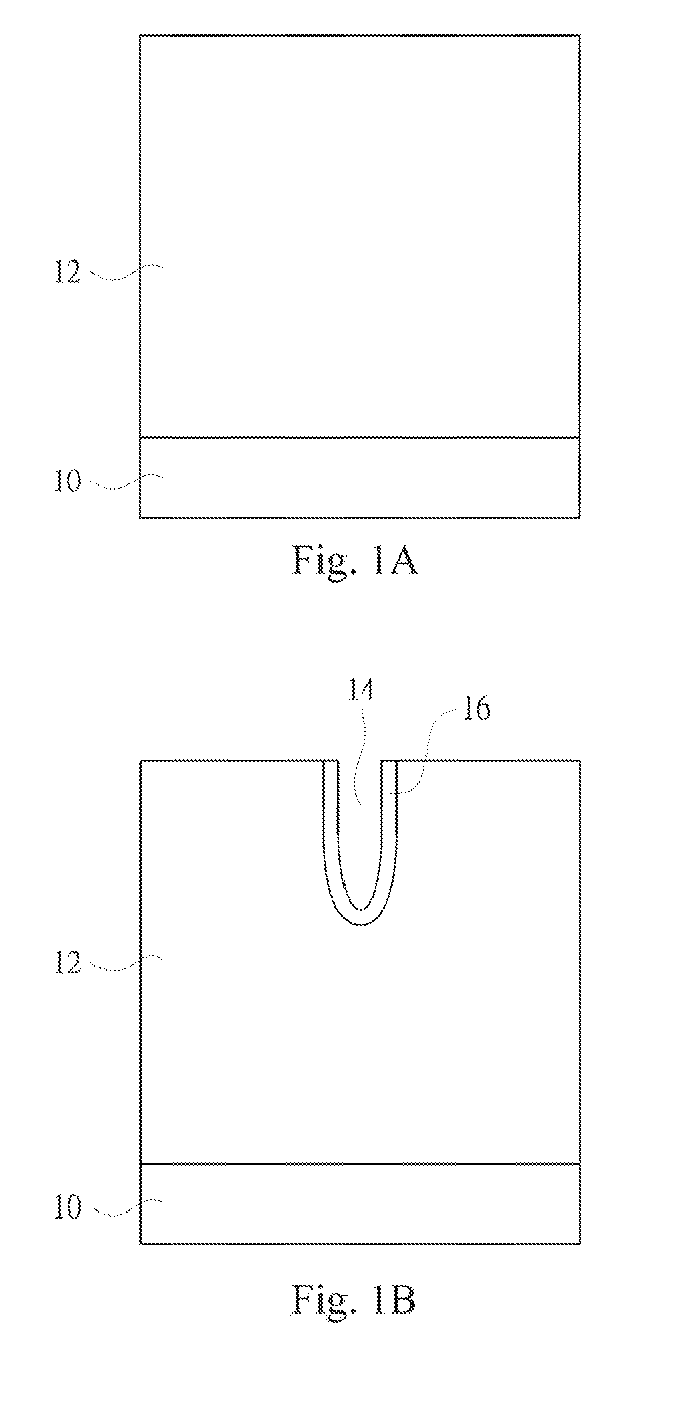
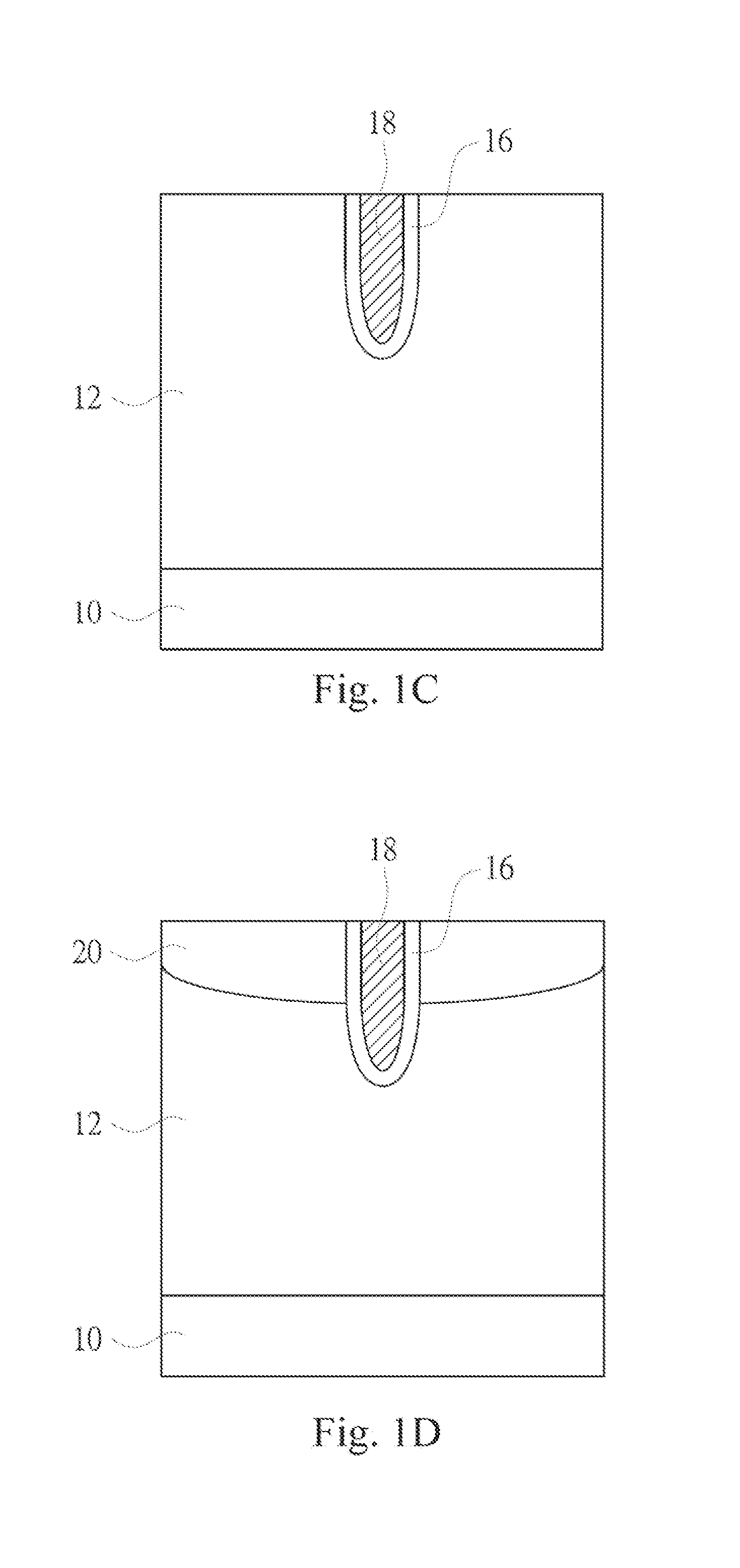
[0028]FIG. 1A to FIG. 1J shows the fabrication method of the trench power MOSFET structure in accordance to an exemplary embodiment of present disclosure. This embodiment shows the application...


PUM


Abstract

A trench power MOSFET structure and fabrication method thereof is provided. The fabrication method comprises following process. First, form an isolating trench. Then, form at least two doped regions around the isolating trench. The doped regions are adjacent and the doping concentrations of two doped regions are different. Form an isolating structure in the isolating trench. Wherein, the junction profiles of the two doped regions are made by ion implantation method for moderate the electric field distribution and decreasing the conduction loss.

Description

RELATED APPLICATIONS[0001]This application claims priority to Taiwan Application Serial Number 102118533, filed May 24, 2013, which is herein incorporated by reference.BACKGROUND[0002]1. Technical Field[0003]The present disclosure relates to a trench power MOSFET structure and the fabrication method thereof in particular to the trench power MOSFET structure with the two doped regions which's junction profiles are made repeatedly by ion implantation processes.[0004]2. Description of Related Art[0005]In the power MOSFET application filed, the voltages withstanding capability and low impedance characteristics are the MOSFET important capability indices. In the traditional fabrication method, the junction profile could not be controlled and therefore it could not to manufacture the power MOSFET with better voltages withstanding capability and low impedance characteristics.SUMMARY[0006]The present disclosure provides a fabrication method of the trench power MOSFET structure, which compri...

Claims


Application Information

Patent Timeline
Patent Type & Authority Patents(United States)
IPC IPC(8): H01L29/78H01L29/66H01L21/762
CPCH01L29/7827H01L21/76237H01L29/66666H01L21/26513H01L21/26586H01L29/0634H01L29/0649H01L29/0878H01L29/1095H01L29/41766H01L29/66727H01L29/66734H01L29/7813
Inventor HSU, HSIU-WENYEH, CHUN-YINGLEE, YUAN-MING
Owner SUPER GROUP SEMICON
Why Eureka
Try Eureka