Extended landing pad substrate package structure and method

a technology of landing pad and substrate, applied in the field of electronic components, can solve the problems of fundamental restrictions on the ability to minimize the feature size of the substrate, and achieve the effect of minimizing the width of the blind via aperture at the upper surface of the dielectric layer and the length of the blind via apertur

Active Publication Date: 2014-10-28
AMKOR TECH SINGAPORE HLDG PTE LTD
View PDF183 Cites 7 Cited by
  • Summary
  • Abstract
  • Description
  • Claims
  • Application Information

AI Technical Summary

Benefits of technology

[0009]Blind via apertures are formed through an upper circuit pattern embedded into the upper surface of the dielectric layer, through the dielectric layer and to the extended landing pads. The length of the blind via apertures is minimized due to the increased second thickness of the extended landing pads as compared to the first thickness of traces. Accordingly, the width of the blind via apertures at the upper surface of the dielectric layer is minimized. Accordingly, extremely small blind via apertures are formed even when the dielectric layer is relatively thick. This enables the upper circuit pattern to be formed with minimum feature size.

Problems solved by technology

The relatively large width of the blind via apertures at the upper circuit pattern places fundamental restrictions on the ability to minimize the feature size of the substrate.

Method used


Image

  • Extended landing pad substrate package structure and method
  • Extended landing pad substrate package structure and method
  • Extended landing pad substrate package structure and method

Examples


Embodiment Construction

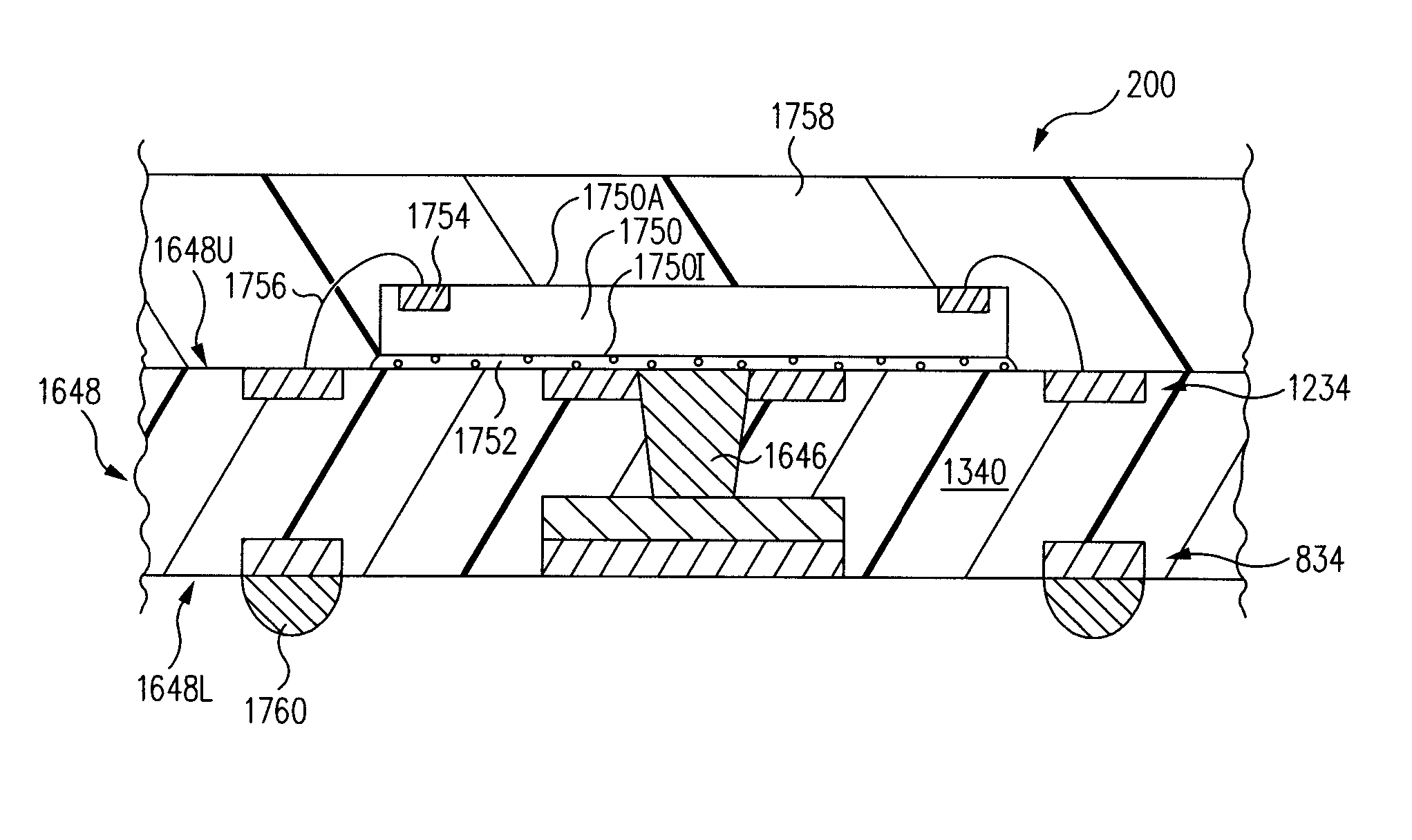
[0020]As an overview, referring to FIG. 15, an extended landing pad substrate package 200 includes a dielectric layer 1340 having an upper surface 1340U and an opposite lower surface 1340L. A lower circuit pattern 834 is embedded in lower surface 1340L of dielectric layer 1340. Lower circuit pattern 834 includes traces 418 having a first thickness T1 and extended landing pads 732 having a second thickness T2 greater than first thickness T1.

[0021]Blind via apertures 1544 are formed through an upper circuit pattern 1234 embedded into upper surface 1340U of dielectric layer 1340, through dielectric layer 1340 and to extended landing pads 732. The length L1 of blind via apertures 1544 is minimized due to the increased thickness T2 of extended landing pads 732 as compared to thickness T1 of traces 418. Accordingly, the width W3 of blind via apertures 1544 at upper surface 1340U of dielectric layer 1340 is minimized. Accordingly, extremely small blind via apertures 1544 are formed even wh...


PUM


Abstract

An extended landing pad substrate package includes a dielectric layer having an upper surface and an opposite lower surface. A lower circuit pattern is embedded in the lower surface of the dielectric layer. The lower circuit pattern includes traces having a first thickness and extended landing pads having a second thickness greater than the first thickness. Blind via apertures are formed through an upper circuit pattern embedded into the upper surface of the dielectric layer, through the dielectric layer and to the extended landing pads. The length of the blind via apertures is minimized due to the increase second thickness of the extended landing pads as compared to the first thickness of traces. Accordingly, the width of the blind via apertures at the upper surface of the dielectric layer is minimized.

Description

BACKGROUND OF THE INVENTION[0001]1. Field of the Invention[0002]The present application relates to the field of electronics, and more particularly, to methods of forming electronic component packages and related structures.[0003]2. Description of the Related Art[0004]During fabrication of an electronic component package substrate, an upper circuit pattern is formed on or embedded within an upper surface of a dielectric layer. Similarly, a lower circuit pattern is formed on or embedded within a lower surface of the dielectric layer.[0005]To electrically interconnect the upper circuit pattern with the lower circuit pattern through the dielectric layer, blind via apertures are formed through the upper circuit pattern and the dielectric layer to expose portions of the lower circuit pattern. The blind via apertures are filled with electrically conductive material to form blind vias electrically interconnecting the upper circuit pattern with the lower circuit pattern.[0006]The blind via a...

Claims


Application Information

Patent Timeline
Patent Type & Authority Patents(United States)
IPC IPC(8): H01L23/12
CPCH01L21/486H01L21/6835H01L23/16H01L23/48H01L23/49827H01L2221/68345H01L2224/131H01L2224/16227H01L2224/2919H01L2224/32225H01L2224/48227H01L2224/73204H01L2224/73265H01L2924/00014H01L2224/16225H01L2224/45099H01L2924/014H01L2924/00H05K3/0064H05K3/4617H05K2203/041H05K2203/061H05K2203/0703
Inventor HINER, DAVID JONHUEMOELLER, RONALD PATRICK
Owner AMKOR TECH SINGAPORE HLDG PTE LTD
Why Eureka
Try Eureka