Electrical contact probe with compliant internal interconnect

a technology of contact probes and internal interconnects, applied in the field of electric contact probes, can solve the problems of deformation of interconnects and arms that are slightly perpendicular to each other, and achieve the effects of maximizing mechanical compliance, stable contact resistance, and maximizing the compliance of interconnects

Active Publication Date: 2007-08-14
XCERRA
View PDF8 Cites 78 Cited by
  • Summary
  • Abstract
  • Description
  • Claims
  • Application Information

AI Technical Summary

Benefits of technology

[0011]The present invention is an improved electrical contact probe with compliant internal interconnect which has been designed to address the drawbacks of prior probe designs. The purpose of the invention is to provide a compliant electrical interconnect between a printed circuit board (PCB) and the external leads of an integrated circuit (IC) package or other electrical circuit, such as an electronic module, during functional testing of the devices. The probe of the present invention consists of two moving fabricated electrically conductive components with one or more electrically conductive compliant helical springs or compliant non-conductive structures in between the components. The compliance of the interconnect is maximized in order to accommodate mechanical tolerances in the interconnect application. In additional to maximizing the mechanical compliance, the helical spring(s) or compliant non-conductive structures of the contact provide adequate normal force to the part under test and PCB in order to provide electrical contact that maintains stable contact resistance. The overall length of the contact is minimized, in order to maximize high frequency response of the overall connection system thereby minimizing electrical inductance and optimizing the AC electrical transmission path.
[0012]Many compliant interconnect designs that utilize springs as compliant members also use the same spring to provide a biasing force between the moving parts of the interconnect. Some designs use an angle bearing surface to provide a slight offset force between the parts during the compliant stroke of the assembly. This bias action between the components improves electrical connectivity between them, however often also influences the force that the assembly can provide to the IC and PCB in such a way that could degrade the interconnect. The present invention provides a bias between the upper and lower component completely independent of this spring(s) or compliant non-conductive structures that provide the contact force for the device under test. The probe of the present invention consists of four flexible cantilever arms that interconnect with each other. During the deflection of the components during the stroke of the probe, the interlocking cantilever arms are always in intimate contact with the mating arm, as the arms are designed specifically with a slight amount of interference with each other. This interference causes the arms to slightly deflect perpendicularly to the force provided by the springs. The design is such that even if the components are slightly rotated and angled with respect to each other, this perpendicular cantilever normal force always maintains contact at least on one point on each arm. By guaranteeing that intimate contact is always maintained, the overall electrical integrity of the probe is maximized by maintaining stable contact resistance from one end of the assembly to the other.

Problems solved by technology

This bias action between the components improves electrical connectivity between them, however often also influences the force that the assembly can provide to the IC and PCB in such a way that could degrade the interconnect.
This interference causes the arms to slightly deflect perpendicularly to the force provided by the springs.

Method used


Image

  • Electrical contact probe with compliant internal interconnect
  • Electrical contact probe with compliant internal interconnect
  • Electrical contact probe with compliant internal interconnect

Examples


Embodiment Construction

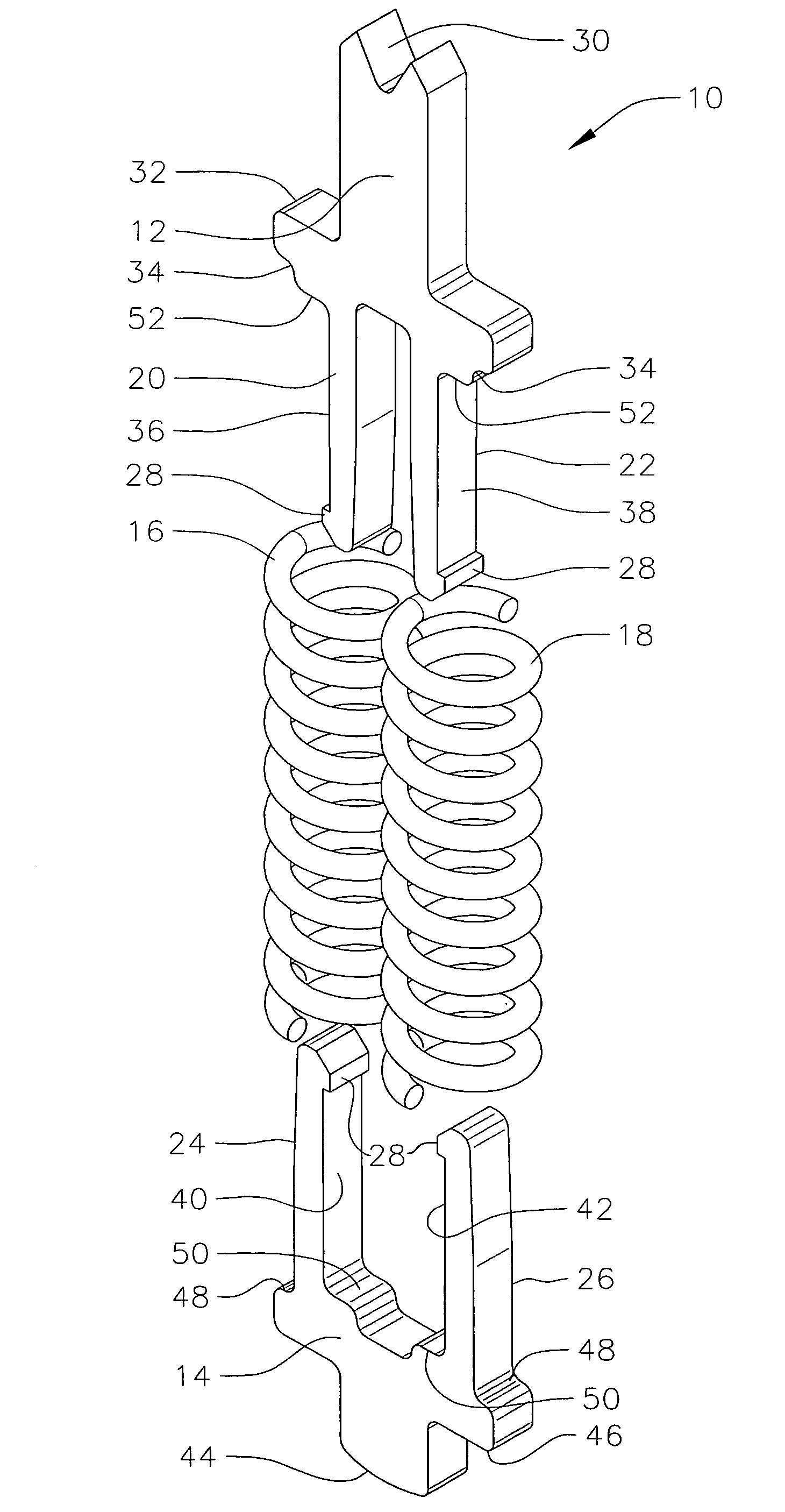
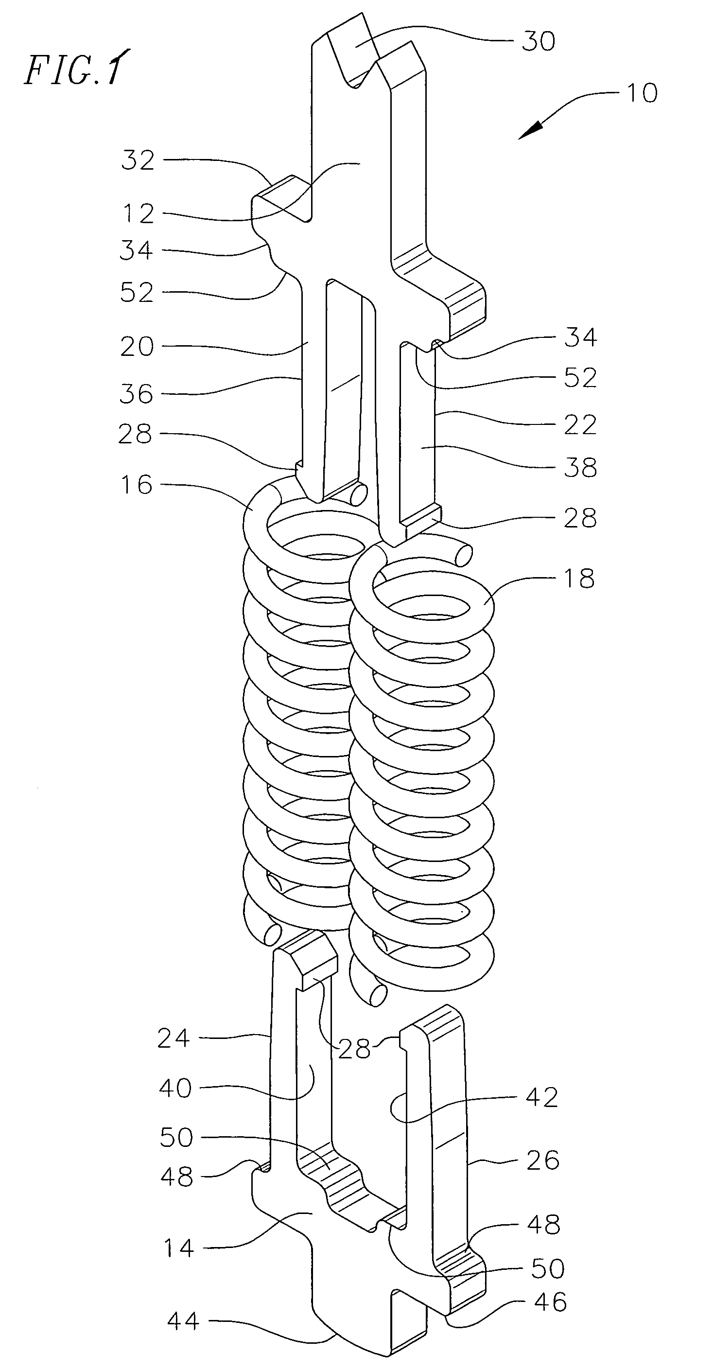
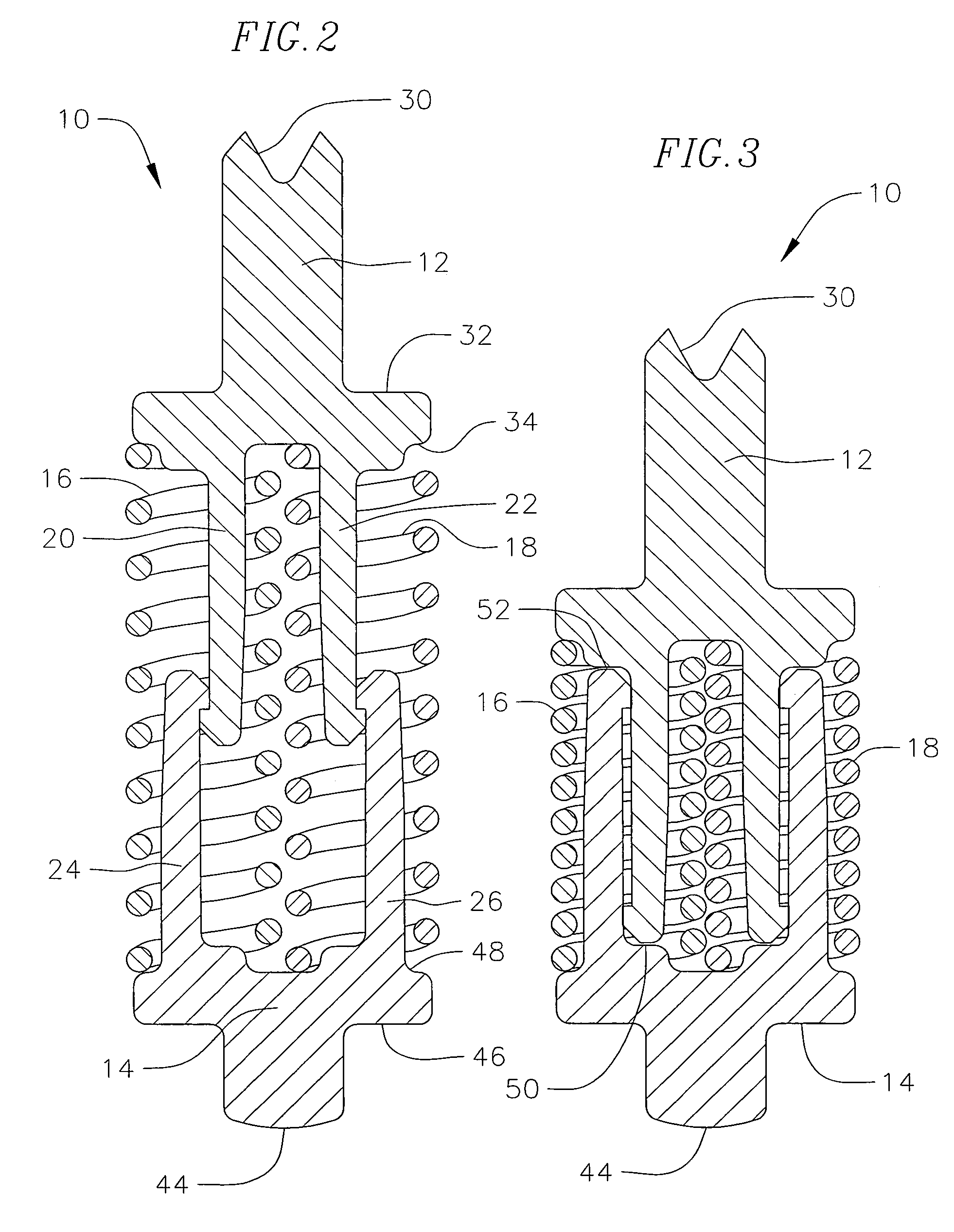
[0028]FIGS. 1-3 illustrate an electrical contact probe 10 with compliant internal interconnect of the present invention. The probe 10 consists of two moving fabricated electrically conductive components, namely upper component or plunger 12 and lower component or barrel 14 with one or more electrically conductive compliant helical springs 16 and 18 in between upper component 12 and lower component 14. The compliance of the interconnect is maximized in order to accommodate mechanical tolerance of the interconnect application. In addition to maximizing the mechanical compliance, the helical springs or other compliant non-conductive structures of the spring probe provide adequate normal force to the unit under test and the printed circuit board between which the spring probe is placed in order to provide electrical contact that maintains stable contact resistance. The overall length of the contact probe is minimized, in order to maximize high frequency response of the overall connectio...


PUM


Abstract

A compliant electrical interconnect having a first component and a second component interlockingly engaged with the first component. Each component has two cantilever arms lockingly engaged and continuously biased against each other. Contact springs are captivated by the cantilever arms providing a contact force for the first and second components.

Description

CROSS-REFERENCE TO RELATED APPLICATION(S)[0001]This application claims the benefit of U.S. Provisional Patent Application No. 60 / 689,755, filed Jun. 10, 2005, the disclosure of which is hereby incorporated by reference herein.FIELD OF THE INVENTION[0002]The present invention relates to electrical contact probes for forming electrical interconnects and, more particularly, to a compliant electrical interconnect between a printed circuit board and the external leads of an integrated circuit package or other electrical circuit, such as an electronic module, during functional testing of the devices.BACKGROUND OF THE INVENTION[0003]Conventional spring-loaded contact probes generally include a moveable plunger, a barrel having an open end for containing an enlarged diameter section or bearing of the plunger, and a spring for biasing the travel of the plunger in the barrel. The plunger bearing slideably engages the inner surface of the barrel. The enlarged bearing section is retained in the...

Claims


Application Information

Patent Timeline
Patent Type & Authority Patents(United States)
IPC IPC(8): G01R31/02
CPCG01R1/0466G01R1/06722G01R1/067
Inventor TREIBERGS, VALTS
Owner XCERRA
Why Eureka
Try Eureka