

3D non-volatile memory device and method of manufacturing the same
a non-volatile memory and non-volatile technology, applied in the field of semiconductor devices, can solve the problems of high difficulty in the foregoing structure of the memory device in the etching process
- Summary
- Abstract
- Description
- Claims
- Application Information
AI Technical Summary
Benefits of technology
Problems solved by technology
Method used
Image

Examples
first embodiment
[0057]FIGS. 4A to 4C are views illustrating a structure of a 3D non-volatile memory device according to the present invention.
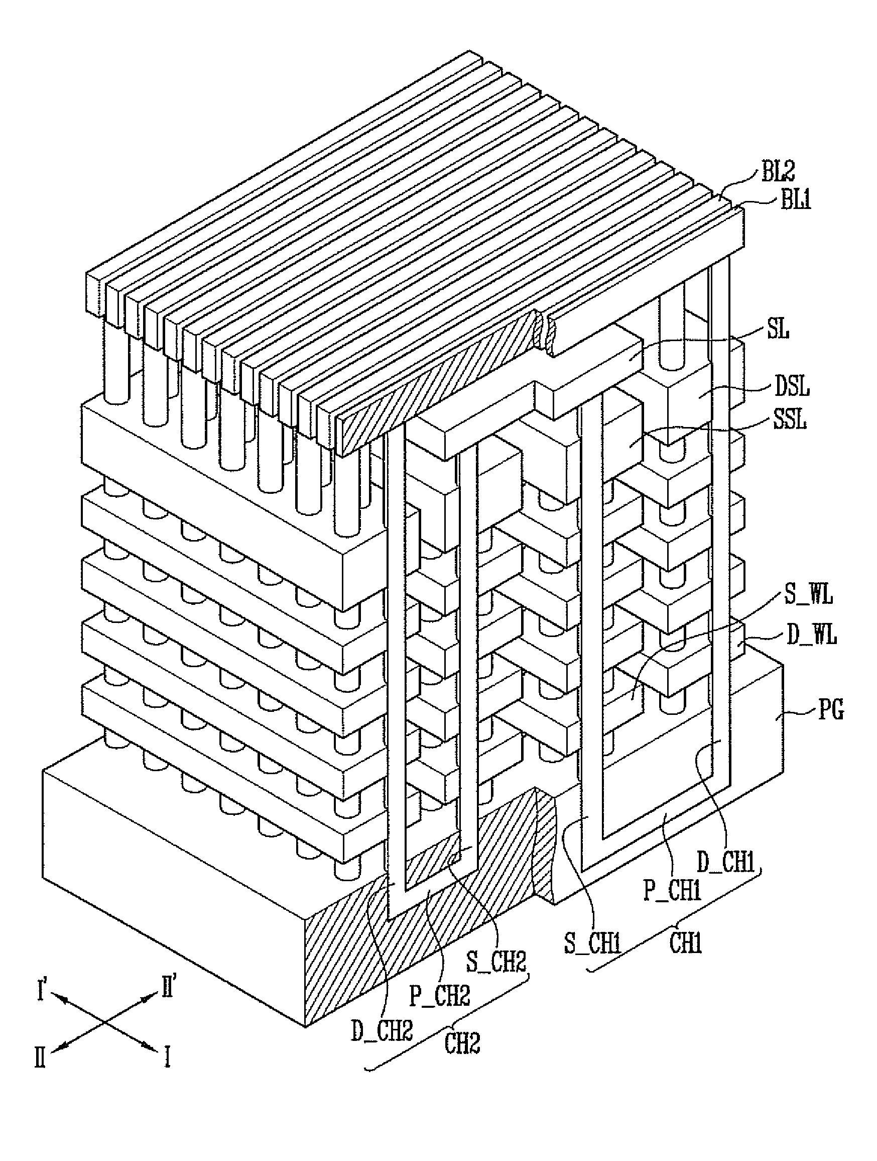
[0058]FIG. 4A is a perspective view of a 3D non-volatile memory device according to a first embodiment of the present invention. As illustrated, the 3D non-volatile memory device includes a pipe gate PG, first channel layers CH1, and the second channel layers CH2. Also, the memory device includes the first to third slits S1˜S3 as described above with reference to FIG. 3D.
[0059]The first channel layers CH1 include a first pipe channel layer P_CH1 buried in the pipe gate PG and a pair of first source side channel layer S_CH1 and first drain side channel layer D_CH1 connected to the first pipe channel layer P_CH1. Also, the second channel layers CH2 include a second pipe channel layer P_CH2 buried in the pipe gate PG and a pair of second source side channel layer S_CH2 and second drain side channel layer D_CH2 connected to the second pipe channel layer P_CH2.
[00...
second embodiment
[0070]FIGS. 5A and 5B are views illustrating a structure of a 3D non-volatile memory device according to the present invention.
[0071]FIG. 5A is a perspective view of a 3D non-volatile memory device according to a second embodiment of the present invention. As illustrated, the memory device includes the first and third slits S1 and S3 as described above with reference to FIG. 3D. Thus, the neighboring source selection lines SSL are connected to each other, and neighboring source side word lines S_WL are connected. Namely, the source selection lines SSL that are positioned on the same layer and neighbor to each other in the second direction II-II′ are connected / formed as a single pattern, and the source side word lines S_WL that are positioned on the same layer and neighbor to each other in the second direction II-II′ are connected as a single pattern. The other structure is the same as that of the first embodiment described above.
[0072]FIG. 5B is a layout view of the 3D non-volatile ...
third embodiment
[0074]FIGS. 6A to 6C are views illustrating a structure of a 3D non-volatile memory device according to the present invention.
[0075]FIG. 6A is a perspective view of a 3D non-volatile memory device according to a third embodiment of the present invention. As illustrated, the 3D non-volatile memory device includes a pipe gate PG, first channel layers CH1, and the second channel layers CH2. Also, the memory device includes the first to fourth slits S1˜S4 as described above with reference to FIG. 3D.
[0076]Source side word lines S_WL and drain side word lines D_WL extending in the first direction I-I′ are stacked over the pipe gate PG and arranged in parallel with each other. Here, the source side word lines S_WL enclose the first source side channel layers S_CH1 of the first channel layers CH1 and the second source side channel layers S_CH2 of the second channel layers CH2. Also, the drain side word lines D_WL enclose the first drain side channel layers D_CH1 of the first channel layers...
PUM
 Abstract
Description
Claims
Application Information