Semiconductor device and manufacturing method of the same

A manufacturing method and semiconductor technology, which are applied in the fields of semiconductor/solid-state device manufacturing, semiconductor devices, and semiconductor/solid-state device components, etc., can solve problems such as reliability reduction, and achieve improved reliability, low reliability suppression, and simple structure. Effect

Inactive Publication Date: 2006-01-18
SANYO ELECTRIC CO LTD
View PDF1 Cites 3 Cited by
  • Summary
  • Abstract
  • Description
  • Claims
  • Application Information

AI Technical Summary

Problems solved by technology

That is, since such a protective layer is not provided, there is a problem in the semiconductor device that the reliability of electronic devices, not shown, etc. on the surface is lowered.

Method used


Image

  • Semiconductor device and manufacturing method of the same
  • Semiconductor device and manufacturing method of the same
  • Semiconductor device and manufacturing method of the same

Examples


Embodiment Construction

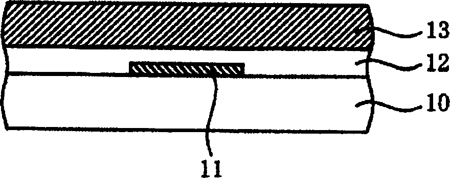
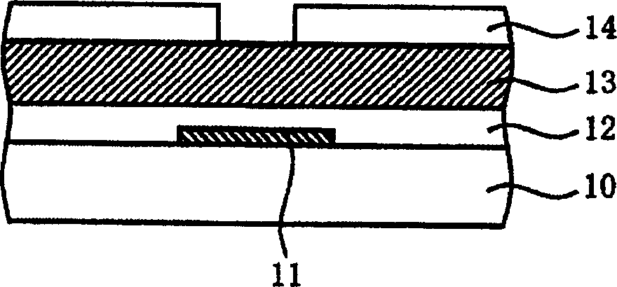
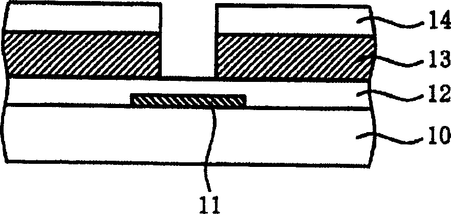
[0057] Next, a semiconductor device according to a first embodiment of the present invention will be described with reference to the drawings. The manufacturing method of the semiconductor device of this embodiment is performed as follows. Figure 1 to Figure 6 It is a sectional view explaining the manufacturing method of the semiconductor device of this embodiment. in addition, Figure 7 is a cross-sectional view illustrating the semiconductor device and its manufacturing method of the present embodiment.

[0058] in addition, Figure 1 to Figure 7 A cross section of the semiconductor substrate 10 is shown at a predetermined boundary between adjacent chips (that is, near a not-shown dicing line) divided by a dicing step described later. in addition, Figure 1 to Figure 7 Among them, electronic devices (not shown) are formed on the surface of the semiconductor substrate 10 . Here, the unillustrated electronic device is, for example, a light-receiving element such as a CCD...


PUM


Abstract

The invention provides a package type semiconductor device and a manufacturing method thereof where reliability is improved without increasing a manufacturing cost. A resin layer and a supporting member are formed on a top surface of a semiconductor substrate formed with pad electrodes. Then, openings are formed penetrating the resin layer and the supporting member so as to expose the pad electrodes. Metal layers are then formed on the pad electrodes exposed in the openings, and conductive terminals are formed thereon. Finally, the semiconductor substrate is separated into semiconductor dice by dicing. When this semiconductor device is mounted on a circuit board (not shown), the conductive terminals of the semiconductor die and external electrodes of the circuit board are electrically connected with each other.

Description

technical field [0001] The present invention relates to a semiconductor device and a manufacturing method thereof, and particularly relates to a packaged semiconductor device and a manufacturing method thereof. Background technique [0002] In recent years, a CSP (Chip Size Package: chip size package) has attracted attention as a packaged semiconductor device. The CSP refers to a small package having an outer dimension substantially the same as that of a semiconductor chip. [0003] Currently, a BGA (Ball Grid Array: Ball Grid Array) type semiconductor device is known as one of CSPs. In this BGA type semiconductor device, a plurality of ball-shaped conductive terminals made of metal members such as solder are arranged in a grid pattern on one main surface of a package, and are electrically connected to a semiconductor chip mounted on the other surface of the package. [0004] Moreover, when this BGA type semiconductor device is incorporated into an electronic device, by pr...

Claims


Application Information

Patent Timeline
Patent Type & Authority Applications(China)
IPC IPC(8): H01L23/48H01L21/60H01L21/78
CPCH01L2224/49175H01L2224/48091H01L2924/01005H01L2224/48465H01L24/32H01L2224/48227H01L24/24H01L2224/023H01L2224/05554H01L2224/24H01L2924/00014H01L2924/00H01L2924/00012H01L2924/0001
Inventor 野间崇
Owner SANYO ELECTRIC CO LTD
Why Eureka
Try Eureka