
Nano-enhanced evanescence integrated technique (NEET) based microphotonic device and sample analysis system

a microphotonic device and integrated technology, applied in the field of microphotonic devices, can solve the problems of high material absorption properties of silicon in the optical spectra, hinder the integration of loc and tas applications, and achieve the effect of increasing the surface binding of bio-specimens

Inactive Publication Date: 2014-11-11
CONCORDIA UNIVERSITY
View PDF4 Cites 2 Cited by
  • Summary
  • Abstract
  • Description
  • Claims
  • Application Information

AI Technical Summary

Benefits of technology

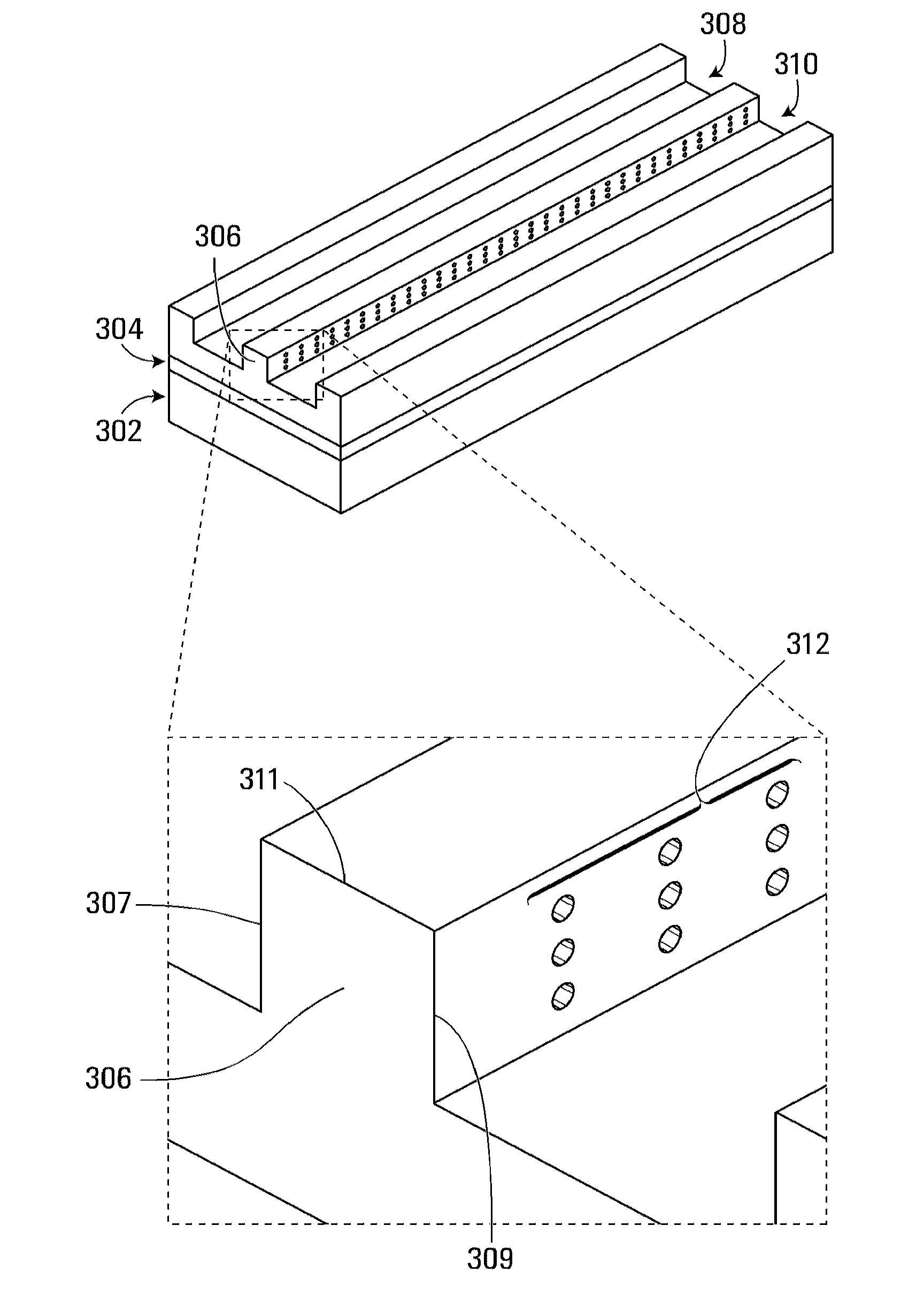
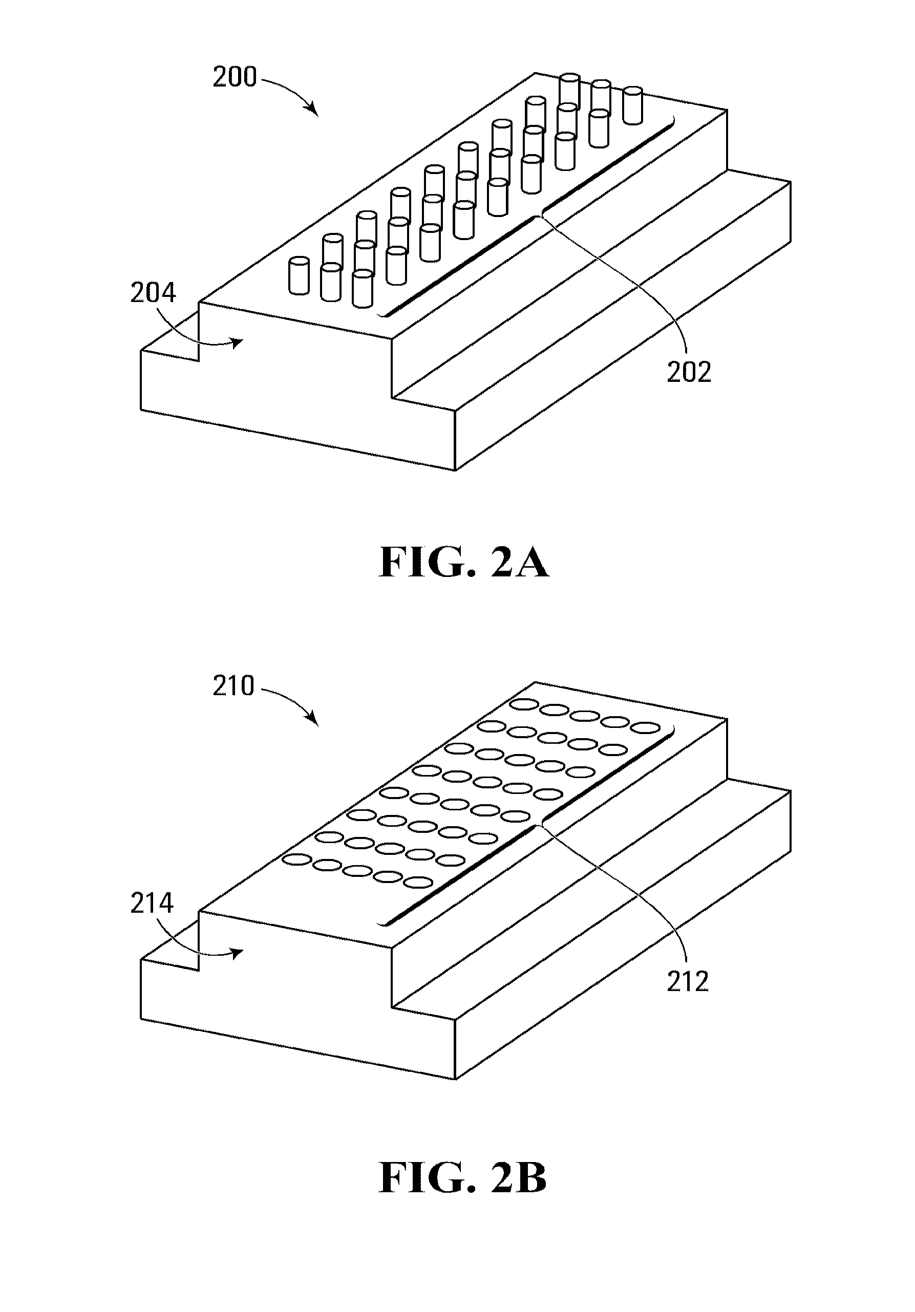
[0008]In some embodiments, the plurality of nanofeatures are formed such that they increase surface binding of bio-specimens on the optical waveguide.

Problems solved by technology

However, for the sake of convenience and the ability to handle smaller sample volumes of chemical and biological species, there are some issues associated with conventional biophotonic based bio-sensing systems, such as miniaturization and portability, that have hindered their integration in LOC and μTAS applications.
However, silicon based platforms typically have two potential drawbacks that can affect biosensor systems, namely, problems with miniaturization and secondly, the typically high material absorption properties of silicon in the optical spectra that are generally used for biosensing, such as the visible and infrared spectra.

Method used


Image

  • Nano-enhanced evanescence integrated technique (NEET) based microphotonic device and sample analysis system
  • Nano-enhanced evanescence integrated technique (NEET) based microphotonic device and sample analysis system
  • Nano-enhanced evanescence integrated technique (NEET) based microphotonic device and sample analysis system

Examples


Embodiment Construction

[0116]In the following detailed description of sample embodiments, reference is made to the accompanying drawings, which form a part hereof, and in which is shown by way of illustration specific sample embodiments in which the present invention may be practiced. These embodiments are described in sufficient detail to enable those skilled in the art to practice the invention, and it is to be understood that other embodiments may be utilized and that logical, mechanical, electrical, and other changes may be made without departing from the scope of the invention. The following detailed description is, therefore, not to be taken in a limiting sense, and the scope is defined by the appended claims.

[0117]Various technical references are referred to herein using numerals in square brackets, [ ]. A complete citation for each of these references is provided at the end of the application.

[0118]Embodiments of the present invention provide a Nano Enhanced Evanescence-integrated Technique (NEET)...


PUM

PropertyMeasurementUnit
angleaaaaaaaaaa
angle of inclinationaaaaaaaaaa
wavelengths wavelengthaaaaaaaaaa

Abstract

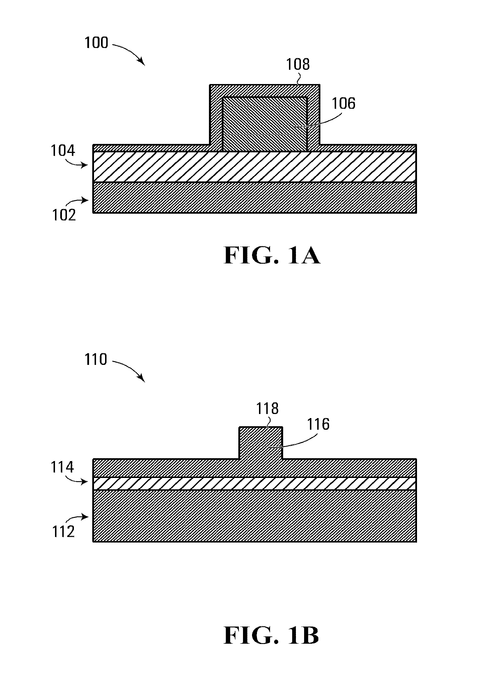
A device, a method of fabricating the device and a sample analysis system that includes the device are provided. The device includes an optical waveguide having a plurality of nanofeatures integrated thereon to influence at least one of evanescence and coupling of an optical field of the optical waveguide. The sample analysis system includes a fluidic actuation system for introducing sample specimen fluid into a microfluidic channel of the device for evanescence based detection.

Description

REFERENCE TO RELATED APPLICATIONS[0001]This application claims the benefit of and is a National Phase Entry of International Application No. PCT / CA2010 / 001429 filed Sep. 16, 2010, and claims the benefit of prior U.S. Provisional Application No. 61 / 242,858 filed Sep. 16, 2009, which are hereby incorporated by reference in their entirety.FIELD OF THE INVENTION[0002]The present invention relates to microphotonic devices, and more specifically to optical waveguide based devices suitable for use as biophotonic sensors.BACKGROUND[0003]Point-Of-Care Testing (POCT) and in-situ solutions to medical diagnosis and biochemical detections are used for early and rapid identification of target specimens.[0004]Biophotonic sensors integrated with complementary Micro-ElectroMechanical Systems (MEMS) integrate optics with biological testing / manipulation for efficient and rapid bio-sensing, thus realizing the concept of Lab-on-a-Chip (LOC) or Micro-Total Analysis Systems (μTAS). However, for the sake o...

Claims


Application Information

Patent Timeline
Patent Type & Authority Patents(United States)
IPC IPC(8): G02B6/122G02B6/00G01N21/00B82Y20/00
CPCB82Y20/00G02B6/1225
Inventor PACKIRISAMY, MUTHUKUMARANCHANDRASEKARAN, ARVIND
Owner CONCORDIA UNIVERSITY
Learn More