Semiconductor device and method for manufacturing the same

a semiconductor and manufacturing method technology, applied in the direction of semiconductor/solid-state device manufacturing, semiconductor devices, electrical appliances, etc., can solve the problems of low performance of semiconductor devices, and achieve the effects of low semiconductor device performance, high crystallinity and high bonding characteristi

Active Publication Date: 2014-11-11
SUMITOMO ELECTRIC IND LTD
View PDF13 Cites 1 Cited by
  • Summary
  • Abstract
  • Description
  • Claims
  • Application Information

AI Technical Summary

Benefits of technology

[0009]Further, according to the method disclosed in PTL 2, since the etching stop layer having unique characteristics is interposed between the underlying layer and the semiconductor layer, crystallinity of n type GaN layer, active layer and p type GaN layer to be grown on the semiconductor layer lowers, resulting in lower performance of the semiconductor device.
[0010]It is an object of the present invention to solve the above-described problem and to provide an n-down type semiconductor device having a semiconductor layer of high crystallinity and high bonding characteristic to a supporting substrate.
[0016]By the present invention, an n-down type semiconductor device having a semiconductor layer of high crystallinity and high bonding characteristic to a supporting substrate can be provided.

Problems solved by technology

Since it is difficult to bond the supporting substrate to the n type semiconductor layer having a rough surface, it is difficult by the methods disclosed in PTLs 1 to 3 to manufacture a n-down type semiconductor device in which an n type semiconductor layer is bonded to a supporting substrate.
Further, according to the method disclosed in PTL 2, since the etching stop layer having unique characteristics is interposed between the underlying layer and the semiconductor layer, crystallinity of n type GaN layer, active layer and p type GaN layer to be grown on the semiconductor layer lowers, resulting in lower performance of the semiconductor device.

Method used


Image

  • Semiconductor device and method for manufacturing the same
  • Semiconductor device and method for manufacturing the same
  • Semiconductor device and method for manufacturing the same

Examples


example 1

[0111]1. Preparation of First Composite Substrate

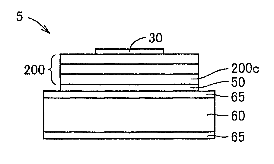
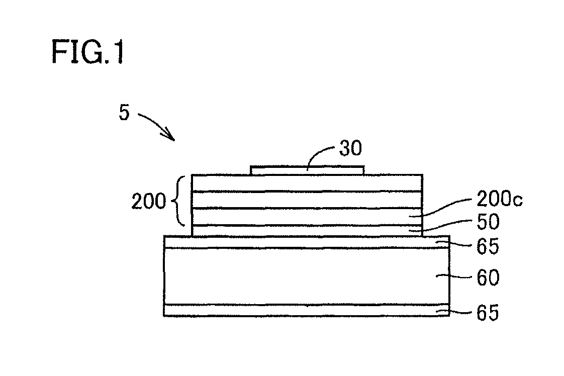
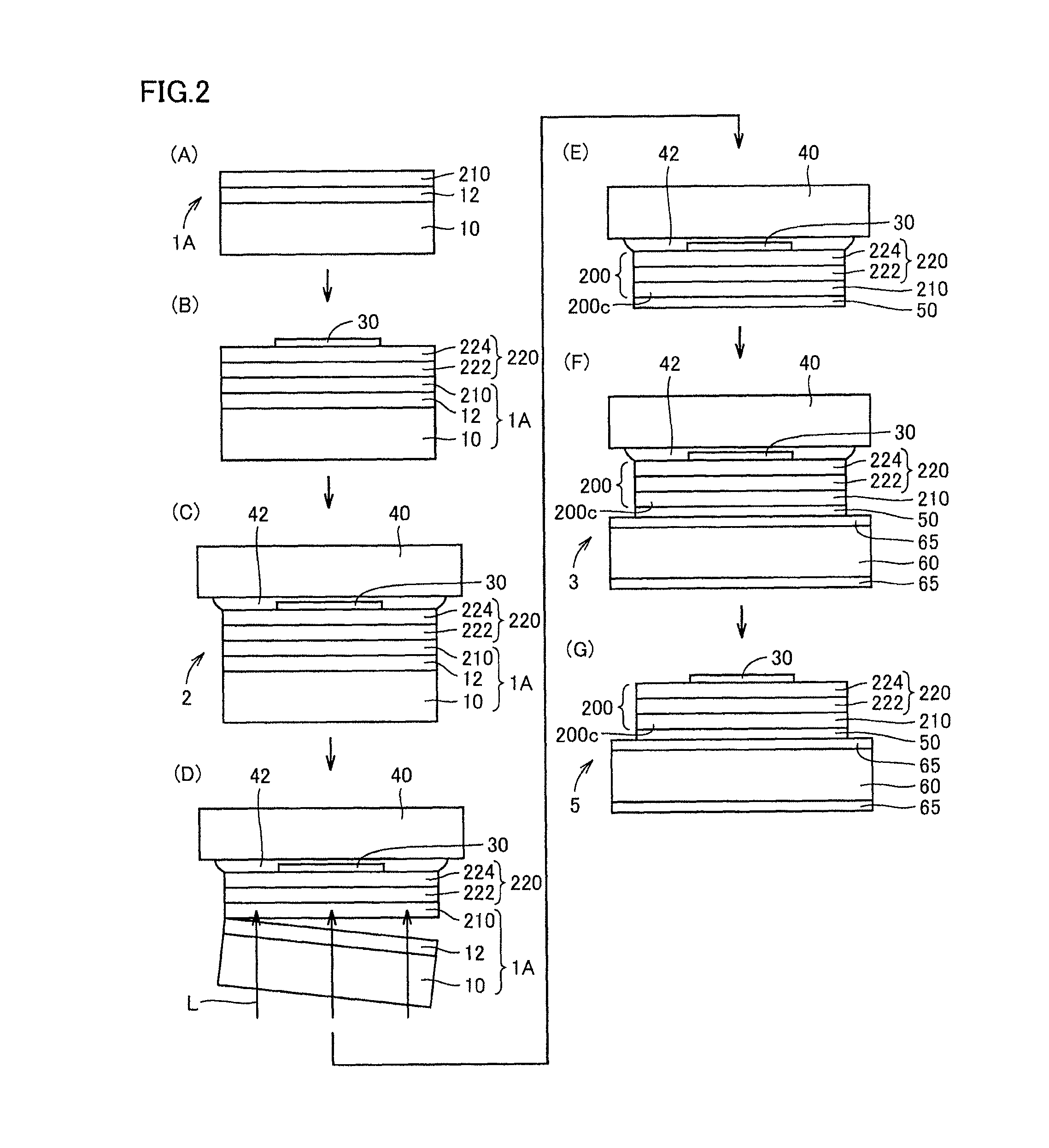
[0112]Referring to (A) of FIG. 2, the first composite substrate 1A was prepared by joining a sapphire underlying substrate (underlying substrate 10) of 2 inches (5.08 cm) in diameter and 400 μm in thickness to a GaN layer (first group III nitride semiconductor layer 210) of 150 nm in thickness, with an SiO2 layer 12 of 200 nm in thickness interposed. Here, the GaN layer (first group III nitride semiconductor layer 210) had dislocation density of 5×106 cm−2 and oxygen concentration of 2×1018 cm−3. The dislocation density was measured by CL (Cathode Luminescence) and the oxygen concentration was measured by SIMS (Secondary Ion Mass Spectroscopy).

[0113]Specifically, the first composite substrate 1A as such was prepared in the following manner. First, referring to FIG. 7(A), on a sapphire underlying substrate (underlying substrate 10) of 2 inches (5.08 cm) in diameter and 40 μm in thickness, SiO2 layer 12a was formed to the thickness of 1...

example 2

[0144]1. Preparation of First Composite Substrate

[0145]Referring to FIG. 3(A), the first composite substrate 1B was prepared by joining a GaN underlying substrate (underlying substrate 10) of 2 inches (5.08 cm) in diameter and 400 μm in thickness to a GaN layer (first group III nitride semiconductor layer 210) of 150 nm in thickness, with a first SiO2 layer 14 of 10 nm in thickness, an amorphous Si layer 16 of 60 nm in thickness and a second SiO2 layer 18 of 230 nm in thickness interposed. Here, the GaN layer (first group III nitride semiconductor layer 210) had dislocation density of 5×106 cm−2 and oxygen concentration of 2×1018 cm−3.

[0146]Specifically, the first composite substrate 1B was prepared in the following manner. First, referring to FIG. 8(A), on a GaN underlying substrate (underlying substrate 10) of 2 inches (5.08 cm) in diameter and 40 μm in thickness, the first SiO2 layer 14 of 10 nm in thickness, amorphous Si layer 16 of 60 nm in thickness, and the second SiO2 layer ...

example 3

[0163]1. From Preparation of First Composite Substrate to Removal of Underlying Layer

[0164]Referring to (A) to (E) of FIG. 4, as in Example 2, the first composite substrate 1B was prepared, the second group III nitride semiconductor layer 220 was grown, temporary underlying layer 40 was joined to form the second composite substrate 2, underlying substrate 10 was removed from the thus formed second composite substrate 2, and then, the first SiO2 layer 14, amorphous Si layer 16 and the second SiO2 layer 18 left on the GaN layer (first group III nitride semiconductor layer 210) were removed by wet etching using a mixed solution of hydrofluoric acid and nitric acid (FIG. 4(E)).

[0165]2. Removal of the First Group III Nitride Semiconductor Layer

[0166]Referring to FIG. 4(F), the GaN layer (first group III nitride semiconductor layer 210) was removed by RIB. The n+ GaN layer 222 exposed by the RIE had extremely high crystallinity as represented by dislocation density of 5×106 cm−2 and oxyge...


PUM

PropertyMeasurementUnit
wavelengthaaaaaaaaaa
thicknessaaaaaaaaaa

Abstract

A semiconductor device includes a supporting substrate, a conductive layer placed on the supporting substrate, and at least one group III nitride semiconductor layer placed on the conductive layer. Of the group III nitride semiconductor layers, a conductive-layer-neighboring group III nitride semiconductor layer has n type conductivity, dislocation density of at most 1×107 cm−2, and oxygen concentration of at most 5×1018 cm−3. Thus, an n-down type device having a semiconductor layer of high crystallinity can be provided.

Description

BACKGROUND OF THE INVENTION[0001]1. Field of the Invention[0002]The present invention relates to a semiconductor device and manufacturing method thereof and, more specifically, to a vertical semiconductor device having superior characteristics and to a method of manufacturing the same. Description of the[0003]2. Background Art[0004]Vertical semiconductor devices, including both light emitting devices and electronic devices, have characteristics that packaging is easy and area efficiency is high. As a method of manufacturing a vertical semiconductor device having such characteristics, a method of joining semiconductor layers grown on an underlying substrate to a supporting substrate different from the underlying substrate has been proposed.[0005]By way of example, Japanese Patent Laying-Open No. 2010-212719 (PTL 1) discloses forming rugged patterns on a surface of a semiconductor layer (a surface of an n type semiconductor layer) after removing an underlying substrate from semiconduc...

Claims


Application Information

Patent Timeline
Patent Type & Authority Patents(United States)
IPC IPC(8): H01L31/0256H01L33/00H01L29/15H01L33/02
CPCH01L33/0079H01L33/025H01L33/007H01L33/0093H01L33/32
Inventor KYONO, TAKASHIISHIHARA, KUNIAKIHACHIGO, AKIHIROYOSHIDA, TAKAHISAUENO, MASAKIKIYAMA, MAKOTO
Owner SUMITOMO ELECTRIC IND LTD
Why Eureka
Try Eureka