
Glitch-free input transition detector

a transition detector and input technology, applied in the field of glitch-free input transition detectors, can solve problems such as signal distortions, noise, etc., and achieve the effects of avoiding signal distortions, signal glitches or timing mismatches that are difficult to detect, and input transition detection circuits that are susceptible to errors

Active Publication Date: 2014-11-18
INTEGRATED SILICON SOLUTION
View PDF2 Cites 3 Cited by
  • Summary
  • Abstract
  • Description
  • Claims
  • Application Information

AI Technical Summary

Benefits of technology

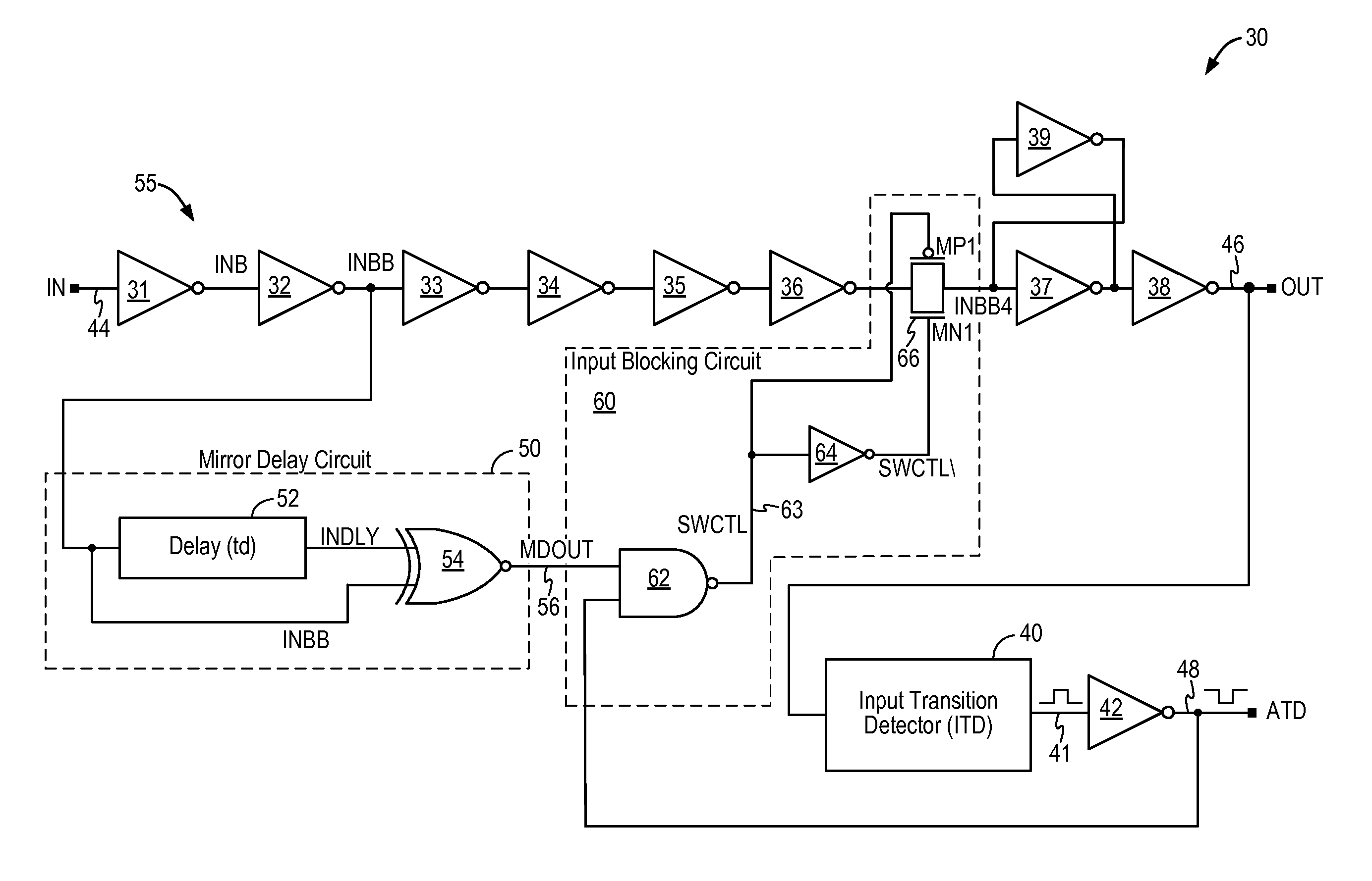
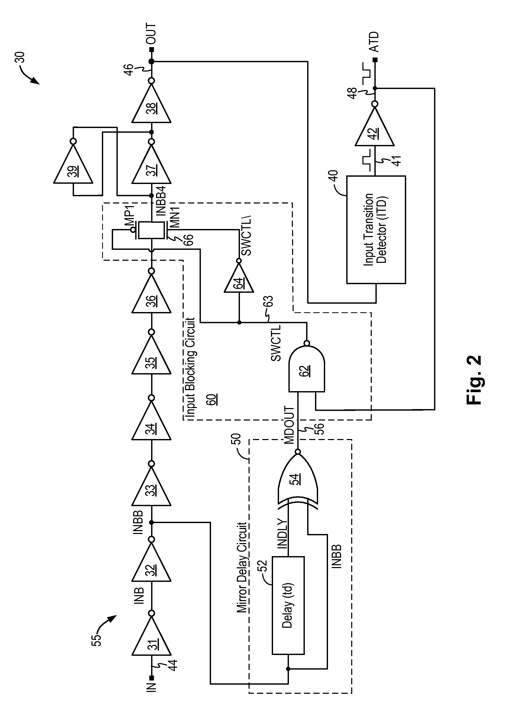
The invention is a circuit and method for detecting signal transitions in electronic systems. The circuit includes a mirror delay circuit and an input blocking circuit to prevent glitches and undesired signal pulses from being passed to the output signal node, resulting in stable and correct transition detection pulses. This prevents signal distortions from being detected as a valid signal transition and ensures normal system operation. The technical effect of the invention is to provide a reliable and accurate input transition detection circuit that prevents glitches from causing erroneous detection pulses and ensures consistent pulse width.

Problems solved by technology

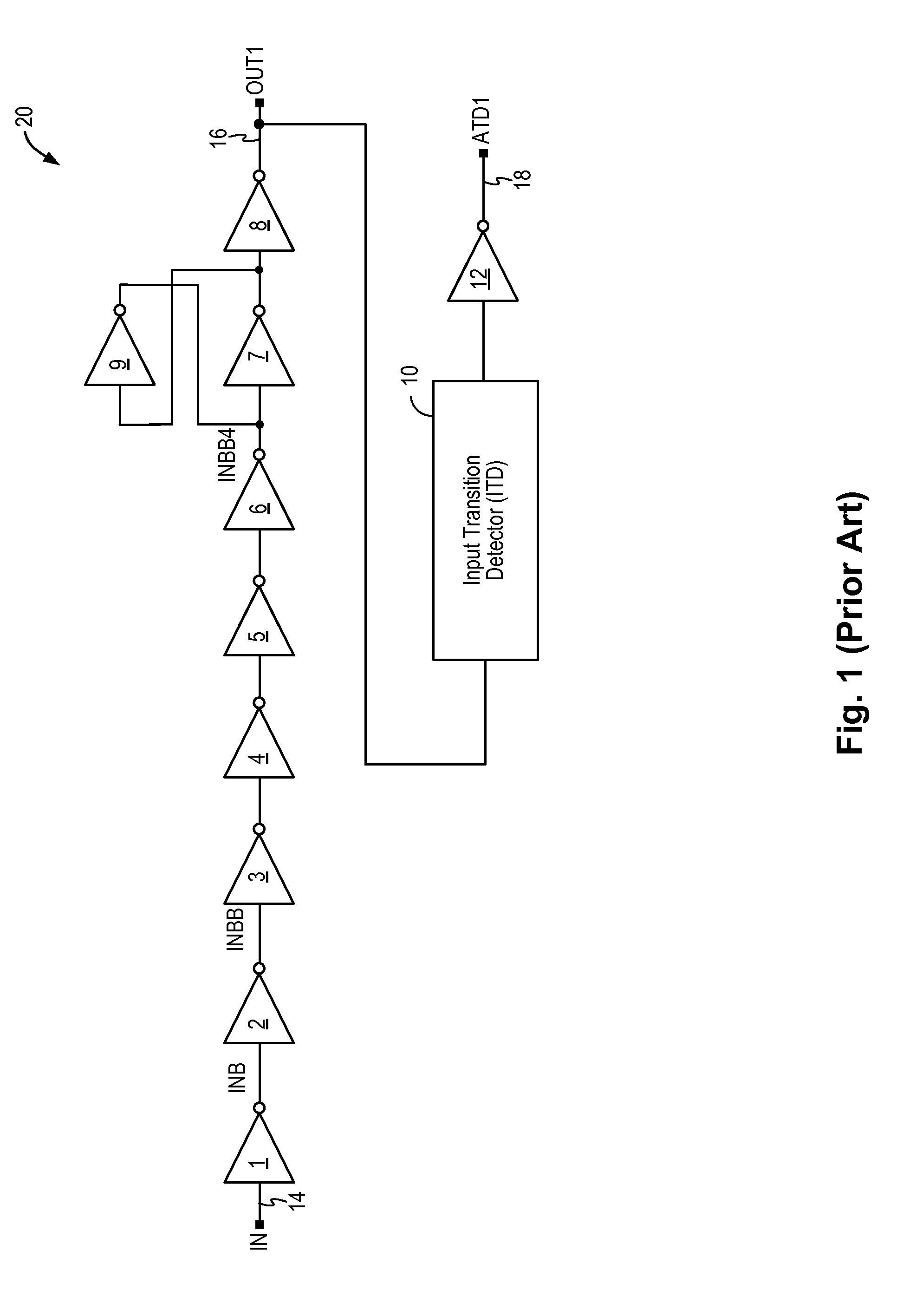
However, in practice, signal distortions, such as noise, signal glitches or timing mismatches, cannot be avoided due to the combination of different electronic components in a system, each with its own functionalities and logic complexities.
Signal glitches are of particular concern as the glitches may be erroneously perceived as a valid input signal to the input circuit of a system.
Signal glitches can be difficult to detect as the glitches are unpredictable and can be very narrow, such as nano or pico second pulse width.
However, these input transition detection circuits are susceptible to error when the input signal is distorted by glitches.
As a result, the detection output signal ATD1 may include erroneous detection pulses, such as causing multiple detection pulses to be generated when there is actually not a valid input transition.

Method used


Image

  • Glitch-free input transition detector
  • Glitch-free input transition detector
  • Glitch-free input transition detector

Examples


Embodiment Construction

[0011]The invention can be implemented in numerous ways, including as a process; an apparatus; a system; and / or a composition of matter. In this specification, these implementations, or any other form that the invention may take, may be referred to as techniques. In general, the order of the steps of disclosed processes may be altered within the scope of the invention.

[0012]A detailed description of one or more embodiments of the invention is provided below along with accompanying figures that illustrate the principles of the invention. The invention is described in connection with such embodiments, but the invention is not limited to any embodiment. The scope of the invention is limited only by the claims and the invention encompasses numerous alternatives, modifications and equivalents. Numerous specific details are set forth in the following description in order to provide a thorough understanding of the invention. These details are provided for the purpose of example and the inv...


PUM


Abstract

A circuit for detecting a signal transition on an input signal includes a mirror delay circuit and an input blocking circuit to prevent signal glitches or undesired signal pulses from being passed to the output signal node, thereby preventing signal distortions from being detected as a valid signal transition. The input transition detection circuit generates stable and correct transition detection pulses having a consistent pulse width.

Description

BACKGROUND OF THE INVENTION[0001]Modern day electronic systems demand very clean power and signal conditions due to high signal sensitivity. However, in practice, signal distortions, such as noise, signal glitches or timing mismatches, cannot be avoided due to the combination of different electronic components in a system, each with its own functionalities and logic complexities. Signal glitches are of particular concern as the glitches may be erroneously perceived as a valid input signal to the input circuit of a system. Signal glitches can be difficult to detect as the glitches are unpredictable and can be very narrow, such as nano or pico second pulse width.[0002]Electronic systems often employ an Input Transition Detection (ITD) circuit, such as an address transition detector (ATD) or a data transition detector (DTD), following the input stage to detect for signal transitions on the input signal. However, these input transition detection circuits are susceptible to error when th...

Claims


Application Information

Patent Timeline
IPC IPC(8): H03K3/013G01R29/02G01R19/165
CPCG01R19/16504H03K3/013H03K5/1534H03K2005/00293G01R19/175H03K2005/00136
Inventor JANG, SEONG, JUN
Owner INTEGRATED SILICON SOLUTION
Learn More