Epoxy-amine underfill materials for semiconductor packages

a technology of underfill materials and semiconductors, applied in the direction of adhesive types, solid-state devices, basic electric elements, etc., can solve the problems of small space between the chip's circuitry and the underlying mounting, and the demand for complex functions of consumer electronics

Inactive Publication Date: 2014-12-23
INTEL CORP
View PDF3 Cites 23 Cited by
  • Summary
  • Abstract
  • Description
  • Claims
  • Application Information

AI Technical Summary

Problems solved by technology

Today's consumer electronics market frequently demands complex functions requiring very intrica...

Method used


Image

  • Epoxy-amine underfill materials for semiconductor packages
  • Epoxy-amine underfill materials for semiconductor packages
  • Epoxy-amine underfill materials for semiconductor packages

Examples


Embodiment Construction

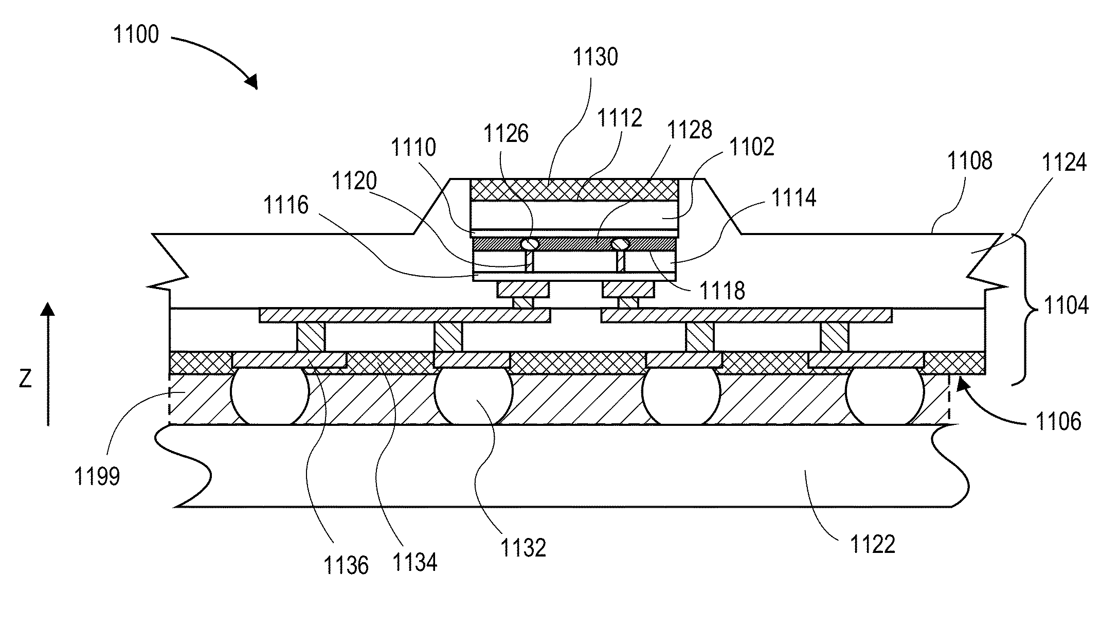
[0019]Epoxy-amine underfill materials for semiconductor packages and semiconductor packages having an epoxy-amine underfill material are described. In the following description, numerous specific details are set forth, such as packaging and interconnect architectures, in order to provide a thorough understanding of embodiments of the present invention. It will be apparent to one skilled in the art that embodiments of the present invention may be practiced without these specific details. In other instances, well-known features, such as specific semiconductor fabrication processes, are not described in detail in order to not unnecessarily obscure embodiments of the present invention. Furthermore, it is to be understood that the various embodiments shown in the Figures are illustrative representations and are not necessarily drawn to scale.

[0020]One or more embodiments of the present invention are directed to low yellow color outgassing underfill materials with improved reliability. Em...


PUM

PropertyMeasurementUnit
Adhesion strengthaaaaaaaaaa

Abstract

Epoxy-amine underfill materials for semiconductor packages and semiconductor packages having an epoxy-amine underfill material are described. In an example, a semiconductor apparatus includes a semiconductor die having a surface with an integrated circuit thereon. A semiconductor package substrate has a surface with a plurality of contact pads thereon. A plurality of conductive contacts couples the surface of the semiconductor die to the surface of the semiconductor package substrate. An epoxy-amine underfill material is disposed between the surface of the semiconductor die and the surface of the semiconductor package substrate and surrounds the plurality of conductive contacts. The epoxy-amine underfill has high adhesion and is based on a low volatility multi-functional amine species.

Description

TECHNICAL FIELD[0001]Embodiments of the invention are in the field of semiconductor packages and, in particular, epoxy-amine underfill materials for semiconductor packages.BACKGROUND[0002]Today's consumer electronics market frequently demands complex functions requiring very intricate circuitry. Scaling to smaller and smaller fundamental building blocks, e.g. transistors, has enabled the incorporation of even more intricate circuitry on a single die with each progressive generation. Semiconductor packages are used for protecting an integrated circuit (IC) chip or die, and also to provide the die with an electrical interface to external circuitry. With the increasing demand for smaller electronic devices, semiconductor packages are designed to be even more compact and must support larger circuit density. Furthermore, the demand for higher performance devices results in a need for an improved semiconductor package that enables a thin packaging profile and low overall warpage compatibl...

Claims


Application Information

Patent Timeline
IPC IPC(8): H01L23/29H01L25/00
CPCH01L2224/32225H01L2224/16225H01L2224/73204H01L25/00H01L23/293H01L2924/15192H01L21/563H01L2924/15311H01L2924/1461H01L2224/1703H01L2224/16145H01L2224/17051C09J163/00H01L23/5385H01L25/0652H01L25/0655H01L2225/06513H01L2225/06517H01L2225/06568H01L2924/00
Inventor XIU, YONGHAOBAI, YIQUNANANTHAKRISHNAN, NISHARARAVIKAR, NACHIKET R.
Owner INTEL CORP
Why Eureka
Try Eureka