Solder ball printing apparatus and solder ball printing method

a printing apparatus and solder ball technology, applied in the direction of soldering apparatus, manufacturing tools,auxillary welding devices, etc., can solve the problems of disadvantageous adhesion and retention of balls on the side faces of pattern holes of masks, difficult to keep flatness, etc., to achieve accurate maintenance of the gap between the mask and the substrate, and maintain the flatness of the substrate

Inactive Publication Date: 2014-12-30
HITACHI LTD
View PDF28 Cites 3 Cited by
  • Summary
  • Abstract
  • Description
  • Claims
  • Application Information

AI Technical Summary

Benefits of technology

[0013]The present invention has been made in view of the above-described problems of the prior art, and an object thereof is to provide a solder ball printing apparatus that reliably and accurately mounts solder balls on a pad on a substrate without positional shifts of the solder balls while keeping the flatness of the substrate and while accurately maintaining a gap between a mask and the substrate. Another object of the present invention is to prevent positional shifts of the solder balls by eliminating the magnetic force at the time of plate separation.
[0016]Further, in the above-described aspect, it is desirable that the members that are provided in the mask absorption portion and can be fitted into the plural hole portions of the substrate mounting table have permanent magnets located on the substrate side and magnetic members located on the side opposite to the substrate, and are installed to hold the positions of the magnets and magnetic pins using only absorption by the magnetic force of the permanent magnets. It is preferable that the second vertically-driving means that drives the mask absorption portion that can be driven independently from the vertical movement of a substrate print table allows the members that are provided in the mask absorption portion and can be fitted into the plural hole portions to be fitted into the hole portions formed in the back surface of the substrate mounting table at the uppermost ascent position of the mask absorption portion, and a mask absorption portion lower-end stopper is provided to prevent the members that can be fitted into the plural hole portions from getting out of the hole portions of the substrate mounting table at the lowermost descent position of the mask absorption portion.
[0018]According to the present invention, the solder ball printing apparatus allows the plural combined members of the permanent magnets and the magnetic members to be fitted into the hole portions on the back surface side of the substrate mounting table on which the substrate is mounted, and the members can be moved up and down by means that is different from substrate mounting table driving means. Thus, the solder balls can be reliably and accurately mounted on a pad (electrode portion) on the substrate without positional shifts of the solder balls while keeping the flatness of the substrate and while accurately maintaining a gap between the mask and the substrate. Further, positional shifts of the solder balls can be prevented by eliminating the magnetic force at the time of plate separation.

Problems solved by technology

If the substrate reception plate is made thinner, the substrate and the substrate reception plate are likely to be absorbed to the mask due to warpage, and thus it is difficult to keep the flatness.
Therefore, if the mask is absorbed by the magnets disposed on the table, it is difficult to allow the mask and the substrate to completely adhere tightly to each other.
Further, when the mask is swiftly separated, the balls mounted on the substrate are flicked, and the balls disadvantageously adhere to and remain on the side faces of the pattern holes of the mask.
However, although the apparatus has a relative difference of the absorption force, the mask is always absorbed, and thus the following troubles are likely to occur.
Therefore, under the circumstance in which the outer diameter of solder balls is reduced every year, it is difficult to stably mount the solder balls.
In addition, the structure of the table becomes complicated and the cost thereof is increased.

Method used


Image

  • Solder ball printing apparatus and solder ball printing method
  • Solder ball printing apparatus and solder ball printing method
  • Solder ball printing apparatus and solder ball printing method

Examples


Embodiment Construction

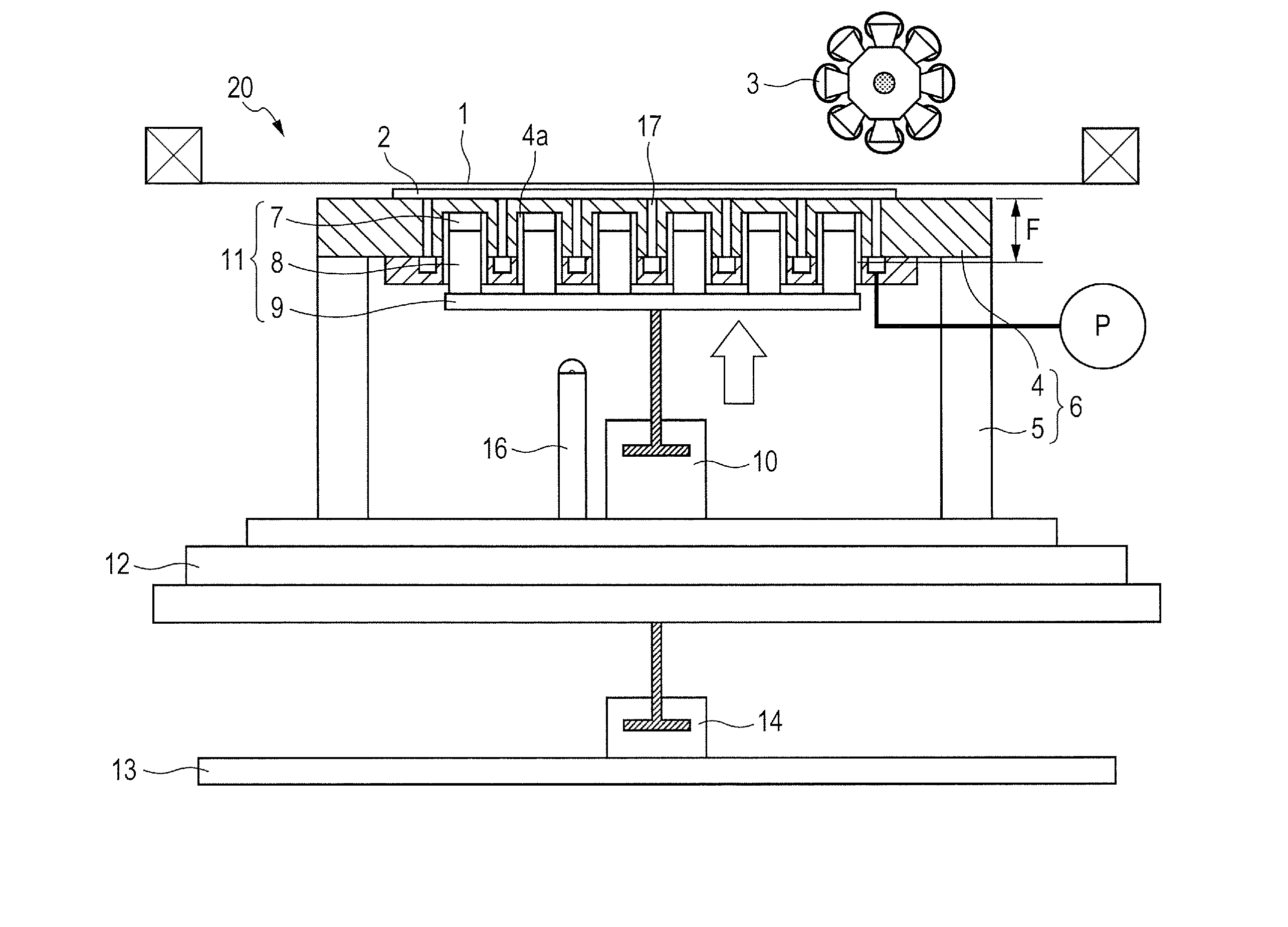
[0028]In a solder ball printing apparatus that prints solder balls on a pad (electrode portion) on a substrate, the pitch of a print target tends to be shortened to as small as 150 μm or smaller. Along with the shortened pitch, solder balls having a size as small as φ20 to φ100 μm are used. Accordingly, an apparatus that can reliably print even small solder balls with a high degree of accuracy is needed. The present invention relates to a solder ball printing apparatus adapted to minute pitches, and some embodiments of the solder ball printing apparatus according to the present invention will be described below using the drawings.

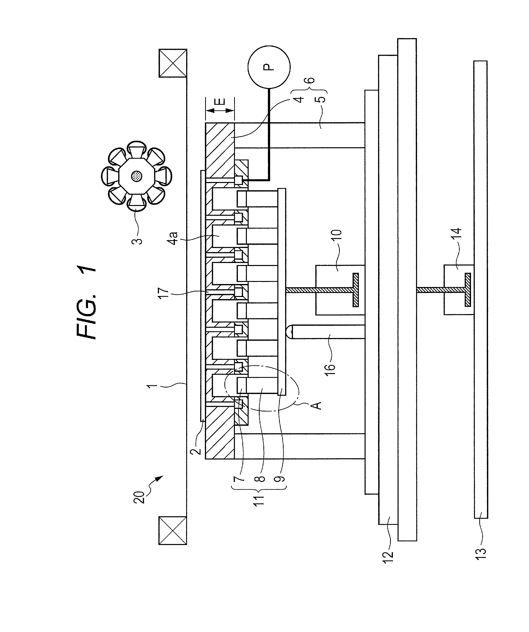
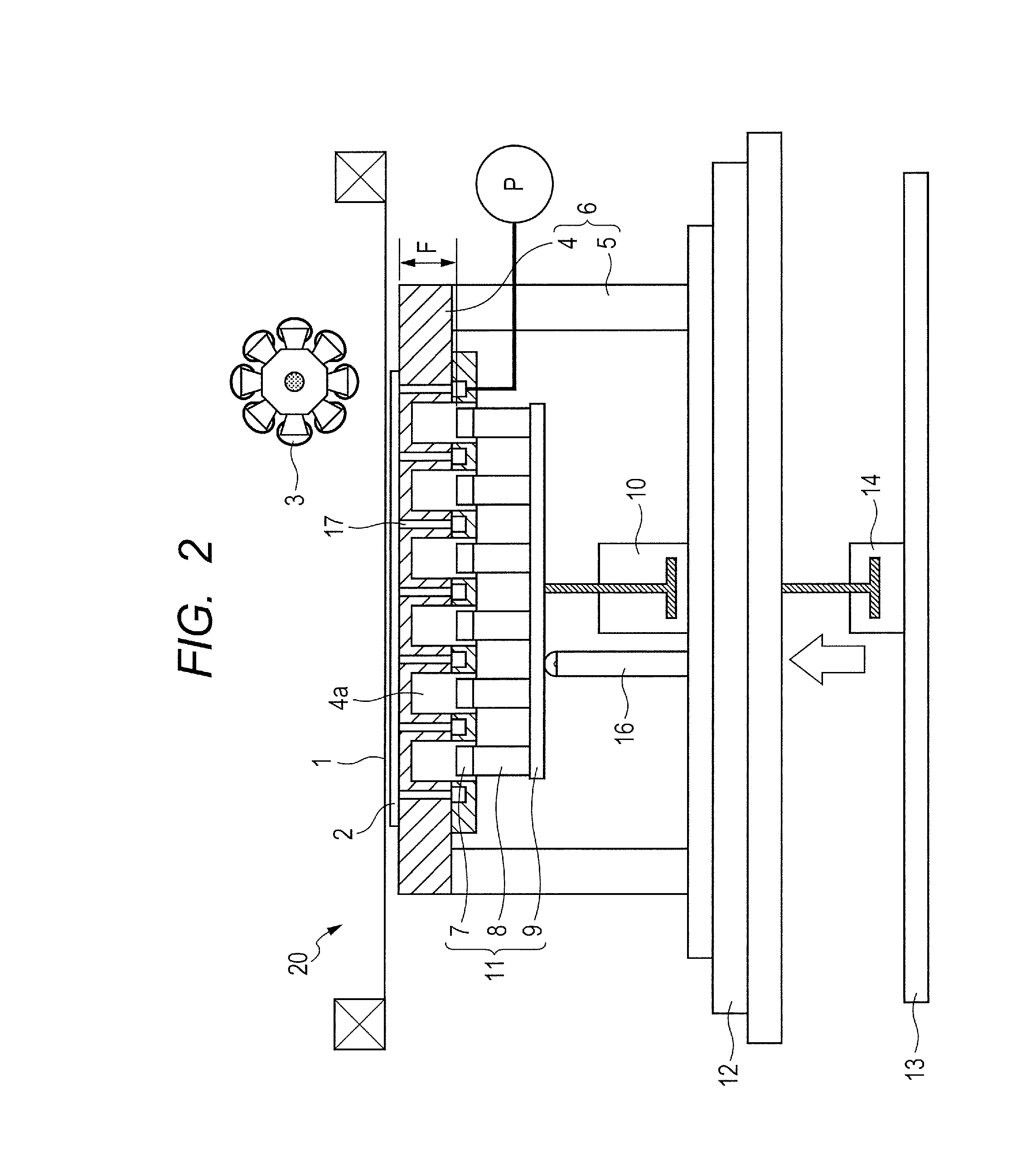
[0029]An embodiment of a solder ball printing apparatus 20 according to the present invention will be described in detail using FIG. 1 to FIG. 7. FIG. 1 is a front part cross-sectional view of the embodiment of the solder ball printing apparatus 20 according to the present invention, and is a view for showing a state in which a substrate 2, to be described ...


PUM

PropertyMeasurementUnit
thicknessaaaaaaaaaa
thicknessaaaaaaaaaa
flatnessaaaaaaaaaa

Abstract

A solder ball printing apparatus fills plural openings formed in a mask with solder balls using a squeegee and prints the solder balls on plural electrode portions formed on a surface of a substrate facing the mask. The solder ball printing apparatus includes: a substrate mounting table on which the substrate is mounted and on the back surface side of which plural hole portions are formed; a print table on which the substrate mounting table is mounted; an XYθ stage which can drive the print table in a horizontal plane; a print table cylinder which can vertically drive the print table; a mask absorption portion which has members that can be fitted into the substrate mounting table; and a mask absorption cylinder which can vertically drive the mask absorption portion.

Description

[0001]The present application claims priority from Japanese Patent Application No. 2013-051692 filed on Mar. 14, 2013, the content of which is hereby incorporated by reference into this application.BACKGROUND OF THE INVENTION[0002]1. Field of the Invention[0003]The present invention relates to a solder ball printing apparatus and a solder ball printing method in which solder balls are printed on electrodes formed on a surface of a substrate.[0004]2. Description of the Related Art[0005]In the case where solder balls are disposed on a mask to fill opening portions of the mask with the solder balls in a conventional solder ball printing apparatus, the magnetic mask is fixed while keeping a gap between the mask and a substrate constant. Therefore, protruding posts are provided on the back surface of the mask, and magnets are provided on the table side across the substrate.[0006]An example of such a solder ball printing apparatus is disclosed in Japanese Patent Application Laid-Open No. ...

Claims


Application Information

Patent Timeline
Patent Type & Authority Patents(United States)
IPC IPC(8): B23K1/20B23K3/06B23K37/00B23K31/02
CPCB23K1/20B23K1/0016B23K2201/42B23K3/087B23K3/0623B23K1/203B23K2101/42
Inventor IGARASHI, AKIOKURIHARA, HIROKUNIMIZUTORI, RYOSUKE
Owner HITACHI LTD
Why Eureka
Try Eureka