System and method for performing scan test

a technology of integrated circuits and scan tests, applied in electronic circuit testing, measurement devices, instruments, etc., can solve problems such as unintentional yield loss

Active Publication Date: 2015-01-13
NXP USA INC
View PDF13 Cites 5 Cited by
  • Summary
  • Abstract
  • Description
  • Claims
  • Application Information

AI Technical Summary

Benefits of technology

[0019]The foregoing has outlined rather broadly the features and technical advantages of the present invention in order that the detailed description of the invention that follows may be better understood. Additional features and advantages of the invention will be described hereinafter, which form the subject of the claims of the invention. It should be appreciated by those skilled in the art that the conception and specific embodiments disclosed may be readily used as a basis for modifying or designing other structures or processes for carrying out the same purposes of the present invention. It should also be realized by those skilled in the art that such equivalent constructions do not depart from the spirit and scope of the invention as set forth in the appended claims.

Problems solved by technology

Thus, the full scan and full memory BIST tests may result in unintentional yield loss.

Method used


Image

  • System and method for performing scan test
  • System and method for performing scan test
  • System and method for performing scan test

Examples


Embodiment Construction

[0011]The detailed description of the appended drawings is intended as a description of the currently preferred embodiments of the present invention, and is not intended to represent the only form in which the present invention may be practiced. It is to be understood that the same or equivalent functions may be accomplished by different embodiments that are intended to be encompassed within the spirit and scope of the present invention.

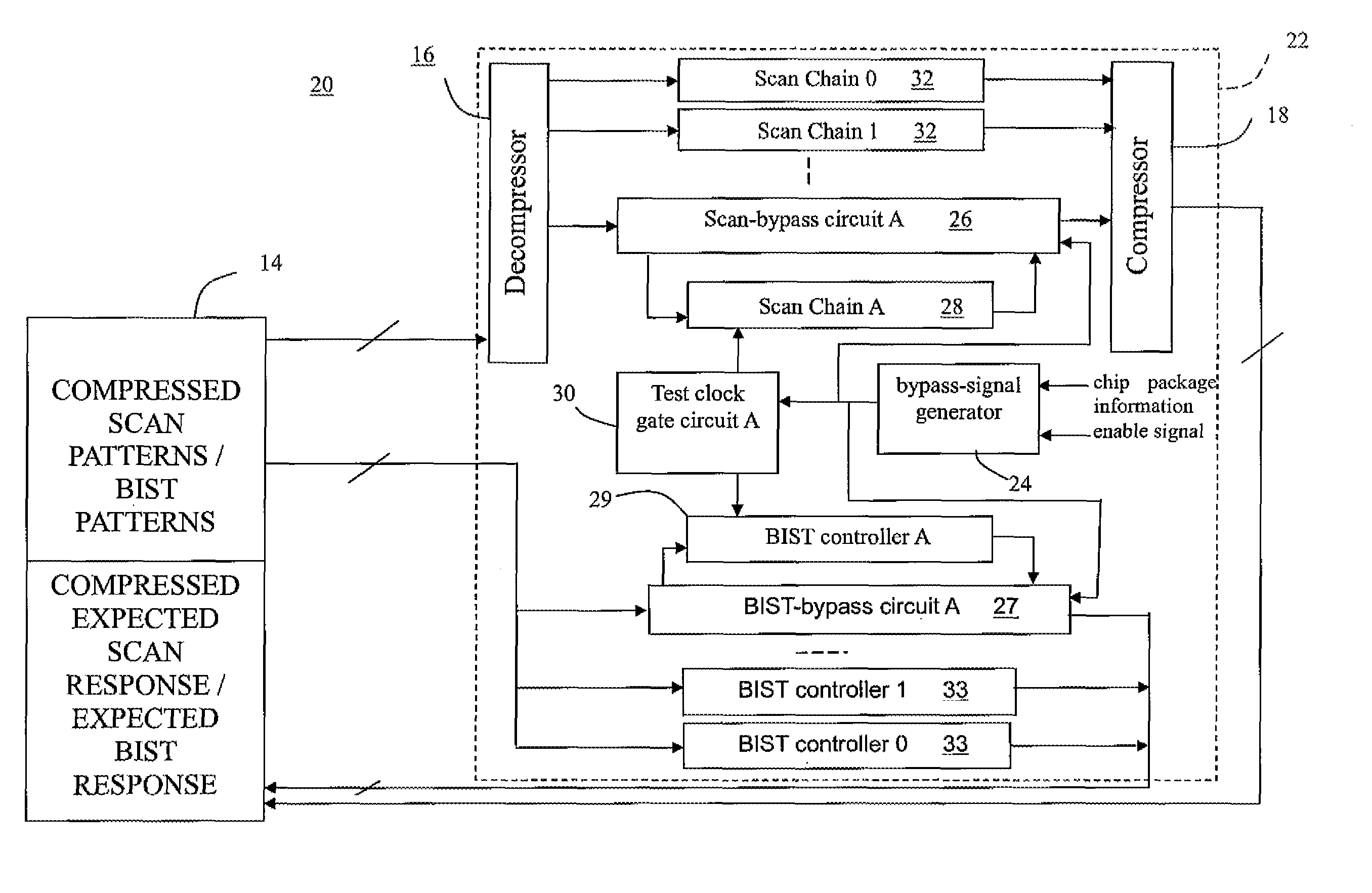
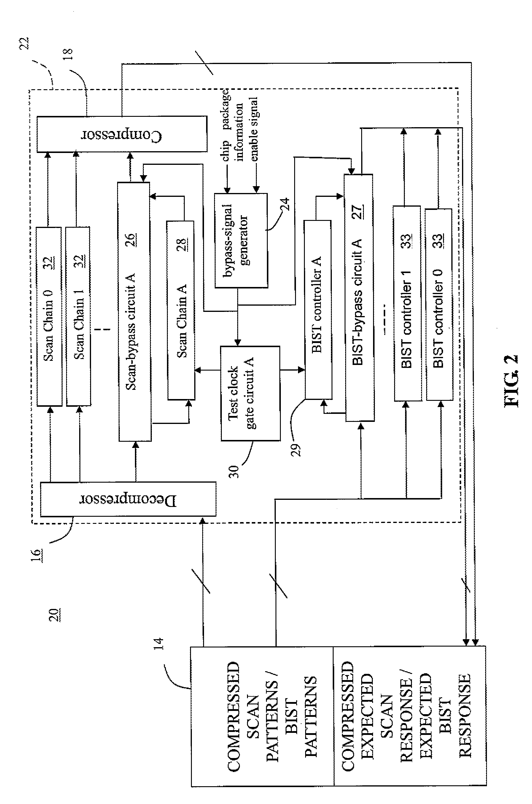
[0012]In one embodiment, the present invention provides a system for performing a scan test that includes a bypass-signal generator and a first scan bypass circuit. The bypass-signal generator generates a first bypass signal based on chip package information. The first bypass signal indicates whether a first scan chain associated with a first non-common IP block of the chip is to be bypassed during the scan test. The first scan bypass circuit bypasses the first scan chain in response to the first bypass signal.

[0013]In another embodiment, the present...


PUM


Abstract

A system for performing a scan test on an integrated circuit such as a System on a Chip (SoC) that may be packaged in different package types and with different features enabled includes a bypass-signal generator and a first scan-bypass circuit. The bypass-signal generator generates a first bypass signal based on chip package information. The first bypass signal indicates whether a first scan chain associated with a first non-common circuit block of the SoC is to be bypassed. The first scan chain is bypassed in response to the first bypass signal. By enabling partial scan testing based on package information, unintentional yield loss caused by a full scan test determining an SoC is faulty can be avoided.

Description

BACKGROUND OF THE INVENTION[0001]The present invention relates generally to scan testing and memory built-in self test (BIST) of integrated circuits and, more particularly, to a system and method for performing a scan test and a memory BIST test on integrated circuits using a scan bypass and a BIST bypass.[0002]In recent years there have been tremendous advancements in the fields of semiconductor devices and electronic circuit integration. Currently, a single system-on-chip (SoC) with multiple package types or options is available. In small package embodiments, certain functional intellectual property (IP) blocks may be masked out depending on the selected package type. The masked out IP blocks may include combinational logic blocks and memory blocks.[0003]FIG. 1 is a schematic diagram illustrating scan testing using scan chain design and memory testing using BIST controllers in system that includes both scan and BIST test systems. That is, scan testing is performed on an integrated...

Claims


Application Information

Patent Timeline
Patent Type & Authority Patents(United States)
IPC IPC(8): G01R31/3177G01R31/3185G01R31/3187G11C29/32
CPCG01R31/318536G11C29/32G11C29/40G01R31/318558G01R31/3187
Inventor WAN, GUOPINGZHANG, SHAYANZHANG, WANGGEN
Owner NXP USA INC
Why Eureka
Try Eureka