Semiconductor device and manufacturing method thereof

a technology of semiconductors and semiconductors, applied in the direction of semiconductor devices, electrical devices, transistors, etc., can solve the problems of affecting the size or profile of the second spacer, the size or profile and the consumption and damage of the first spacer

Active Publication Date: 2015-02-10
UNITED MICROELECTRONICS CORP
View PDF163 Cites 2 Cited by
  • Summary
  • Abstract
  • Description
  • Claims
  • Application Information

AI Technical Summary

Benefits of technology

[0011]According to the manufacturing method for the semiconductor device provided by the present invention, the thermal treatment is introduced to cause a reaction between the carbon-containing layer of the disposal spacer and the first spacer, so that a SiCN-based protecting layer is formed between the carbon-containing layer and the first spacer. Consequently, the SiCN-based protecting layer serves as an etching stop layer during removing the disposal spacer, and thus the underneath first spacer is protected from consumption. Since the first spacer remains unimpaired and impervious to the disposal spacer removal and possesses its original profile due to the SiCN-based protecting layer, the subsequent steps for forming elements such as the second spacer and the source / drain are performed successfully and the obtained second spacer and source / drain can meet the expectation.

Problems solved by technology

For example, it has been found that the first spacer is always consumed and damaged when removing the disposal spacer.
It even damages the profile of the gate structure when removing the disposal spacer.
Furthermore, it is found that the size or profile of the second spacer and the source / drain are all adversely impacted when the first spacer is consumed.
Seriously, it results that the following manufacturing processes fail to meet expectations.

Method used


Image

  • Semiconductor device and manufacturing method thereof
  • Semiconductor device and manufacturing method thereof
  • Semiconductor device and manufacturing method thereof

Examples


Embodiment Construction

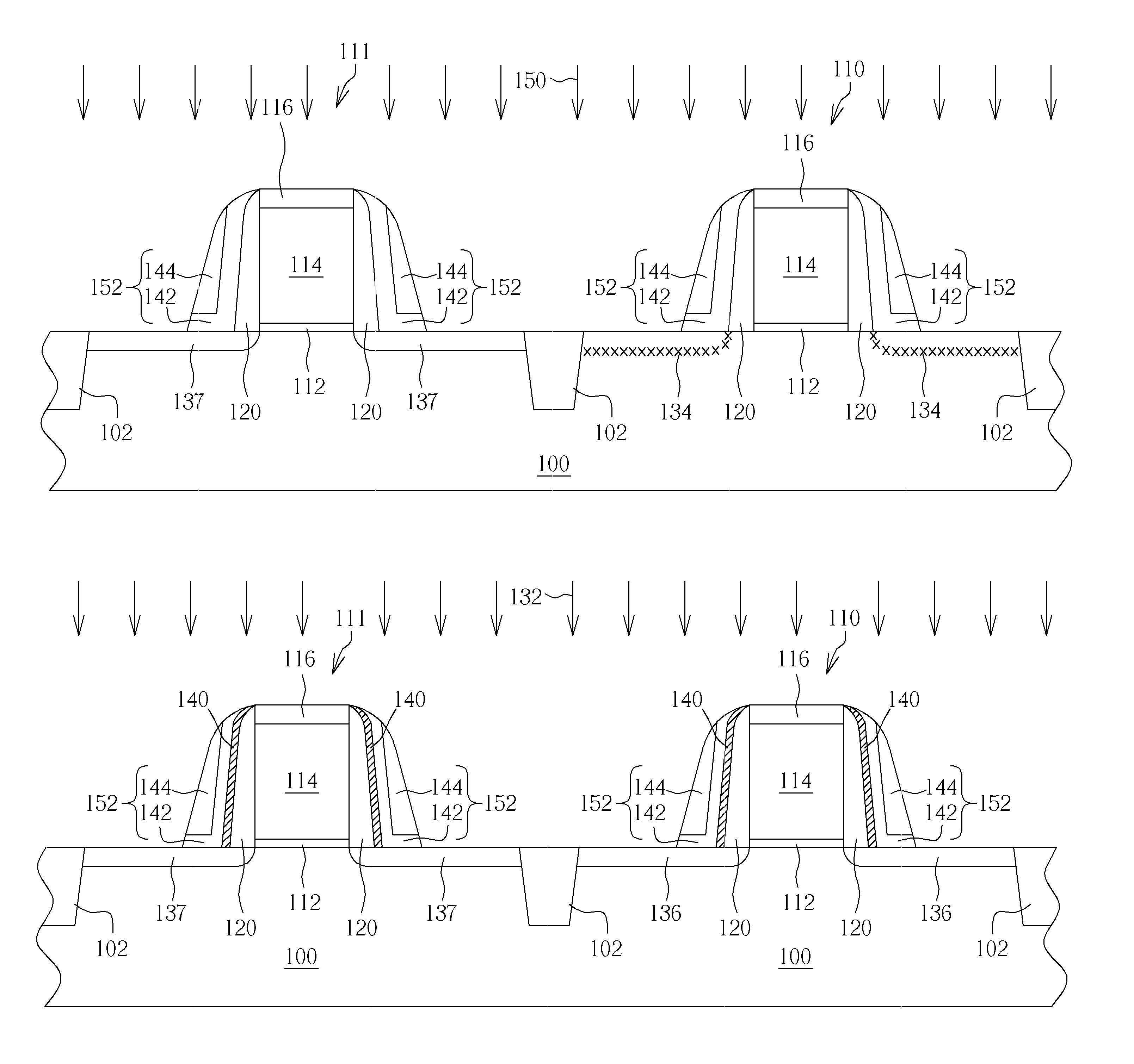
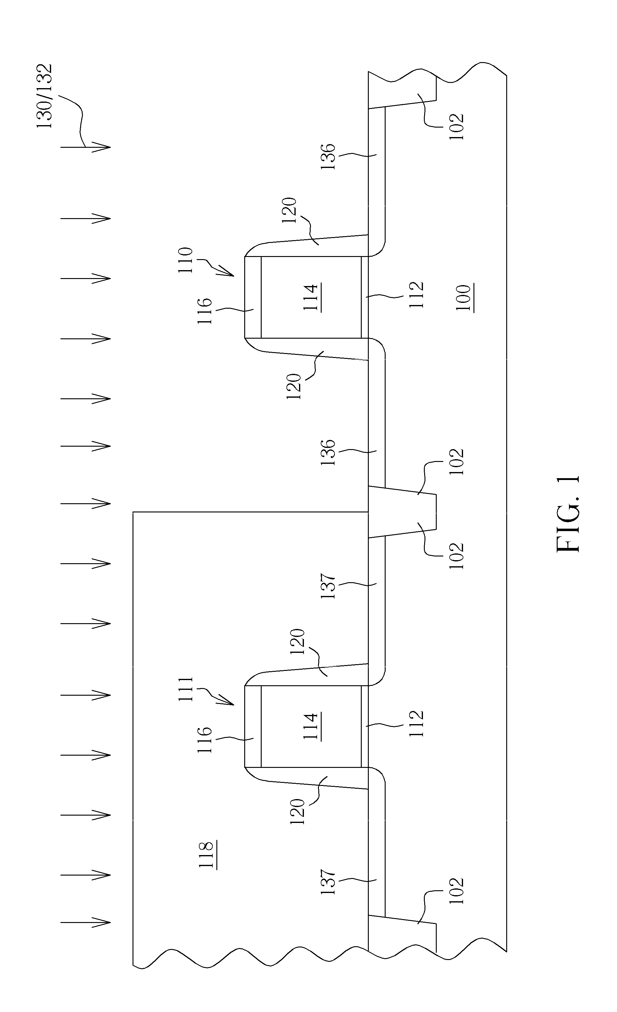
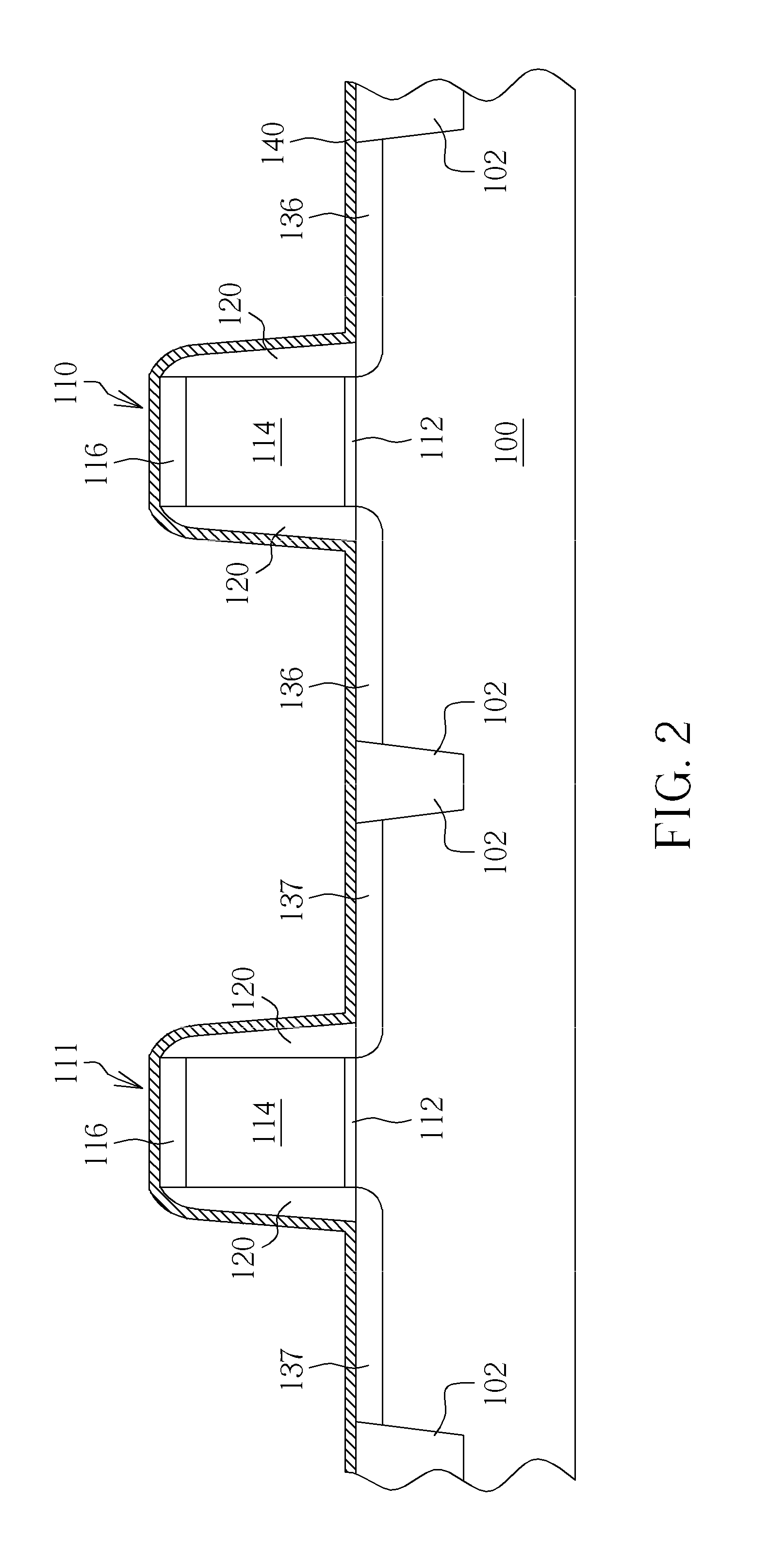
[0042]Please refer to FIGS. 1-4, which are drawings illustrating a manufacturing method for a semiconductor device provided by a first preferred embodiment of the present invention. As shown in FIG. 1, the preferred embodiment first provides a substrate 100 having a plurality of shallow trench isolations (STIs) 102 for providing electrical isolation formed therein. A first gate structure 110 and a second gate structure 111 are formed on the substrate 100. The first gate structure 110 and the second gate structure 111 include a gate dielectric layer 112, a gate conductive layer 114, and a cap layer 116 sequentially and upwardly stacked on the substrate 100. It is well-known to those skilled in the art that the cap layer 116 is formed to cover the gate conductive layer 114 to protect the gate conductive layer 114 from damage that may be caused in any process such as photolithograph process, ion implantation, etching process, or any needed cleaning process in the semiconductor fabricat...


PUM


Abstract

A manufacturing method for a semiconductor device includes providing a substrate having at least a gate structure formed thereon and a first spacer formed on sidewalls of the gate structure, performing an ion implantation to implant dopants into the substrate, forming a disposal spacer having at least a carbon-containing layer on the sidewalls of the gate structure, the carbon-containing layer contacting the first spacer, and performing a thermal treatment to form a protecting layer between the carbon-containing layer and the first spacer.

Description

BACKGROUND OF THE INVENTION[0001]1. Field of the Invention[0002]The invention relates to a semiconductor device and a manufacturing method thereof, and more particularly, to a semiconductor device and a manufacturing method manufacturing method applied with strained-silicon technique.[0003]2. Description of the Prior Art[0004]With semiconductor processes entering the era of the deep submicron meter below 65 nanometer (nm), it has been more and more important to increase the metal-oxide semiconductor (MOS) drive current. To improve device performance, strained-silicon technique such as selective epitaxial growth (hereinafter abbreviated as SEG) method is developed to form epitaxial layers serving as the source / drain of the MOS. Because a lattice constant of the epitaxial layer is different from that of silicon, such characteristic is employed to cause alteration to the band structure of the silicon in the channel region. Accordingly, carrier mobility of the channel region is enhanced...

Claims


Application Information

Patent Timeline
Patent Type & Authority Patents(United States)
IPC IPC(8): H01L21/336
CPCH01L29/7848H01L21/823807H01L21/823814H01L29/165H01L29/6653H01L29/6656H01L29/6659H01L29/66636H01L29/7834
Inventor CHOU, LING-CHUNWANG, I-CHANGHUNG, CHING-WEN
Owner UNITED MICROELECTRONICS CORP
Why Eureka
Try Eureka