
Digital filtering and spread spectrum based interference mitigation for mutual and self capacitance panel

a capacitance panel and digital filtering technology, applied in the field of touch screens, can solve the problems of small signal impact, inability to apply methods to capacitive touch screen systems, and touch screen systems that cannot tolerate extremely small, so as to achieve the effect of determining the capacitance of pixels and reducing interferen

Active Publication Date: 2015-03-03
QUALCOMM INC
View PDF15 Cites 23 Cited by
  • Summary
  • Abstract
  • Description
  • Claims
  • Application Information

AI Technical Summary

Benefits of technology

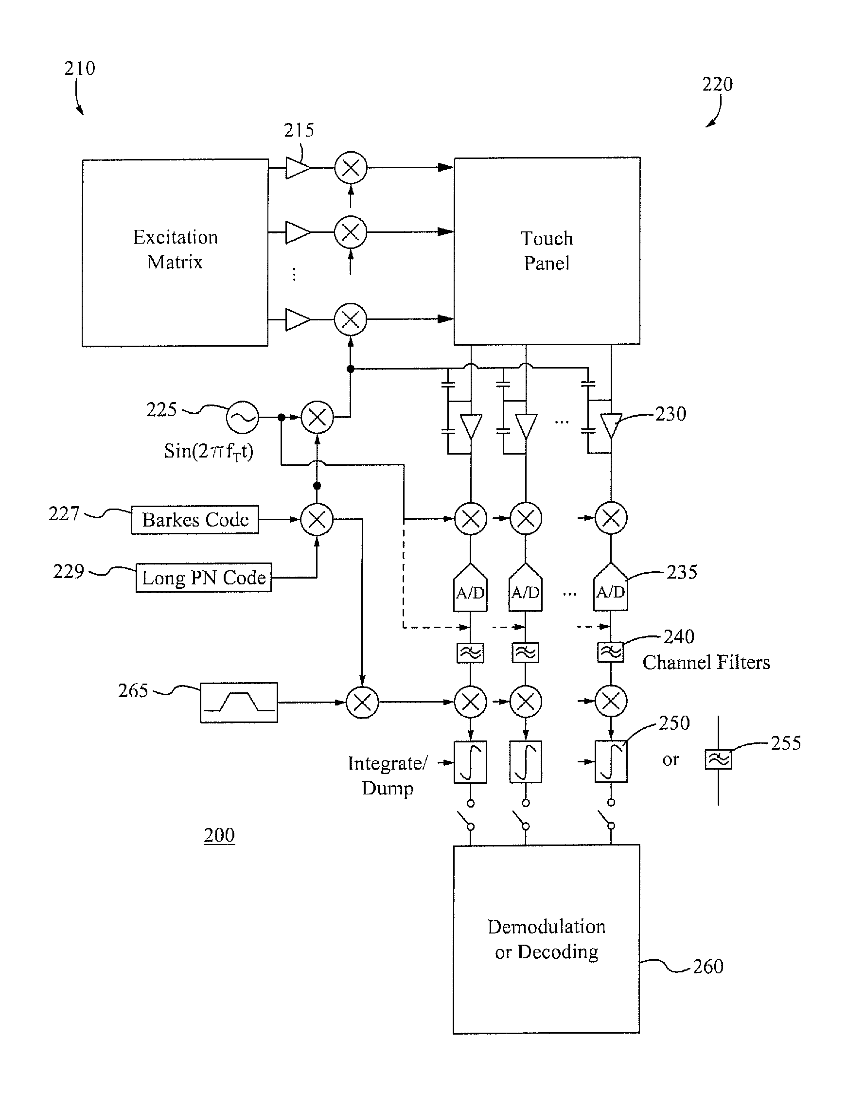
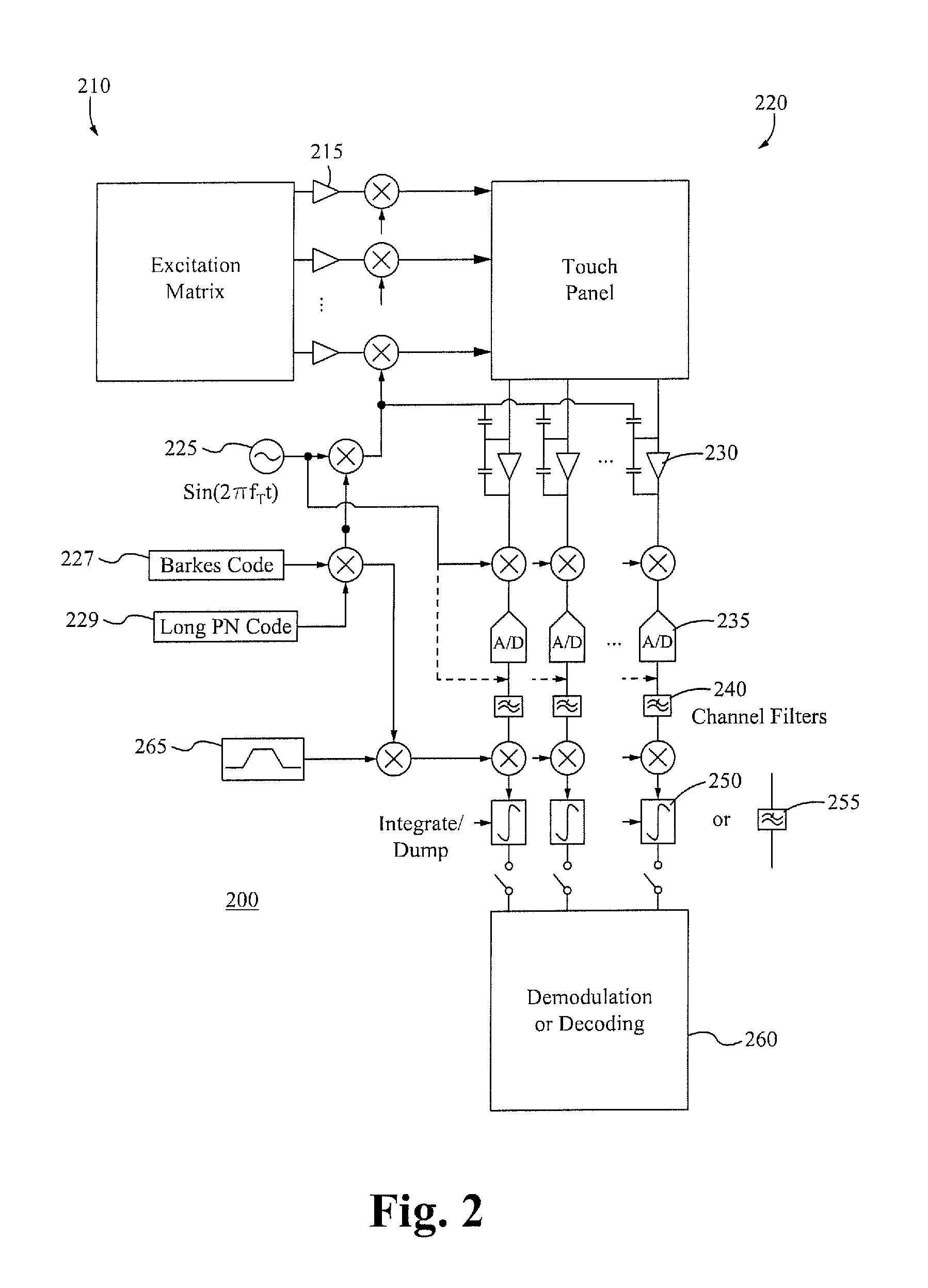
The present invention provides methods for mitigating interference in capacitive touch screen panels using spread spectrum techniques and zero-ISI digital filtering. These techniques have not been previously applied to capacitive touch screen systems, which are more susceptible to interference because the analog signals are stationary and the touch information has a very small impact on the signals. The methods are particularly effective in mitigating touch panel interference and provide a much more accurate touch screen display. Additionally, the invention provides methods of amplifying and filtering the sensed signals using a modified Hadamard matrix and a new approach for determining the capacitance of the pixels. These methods result in a more compact and cost-effective touch screen panel.

Problems solved by technology

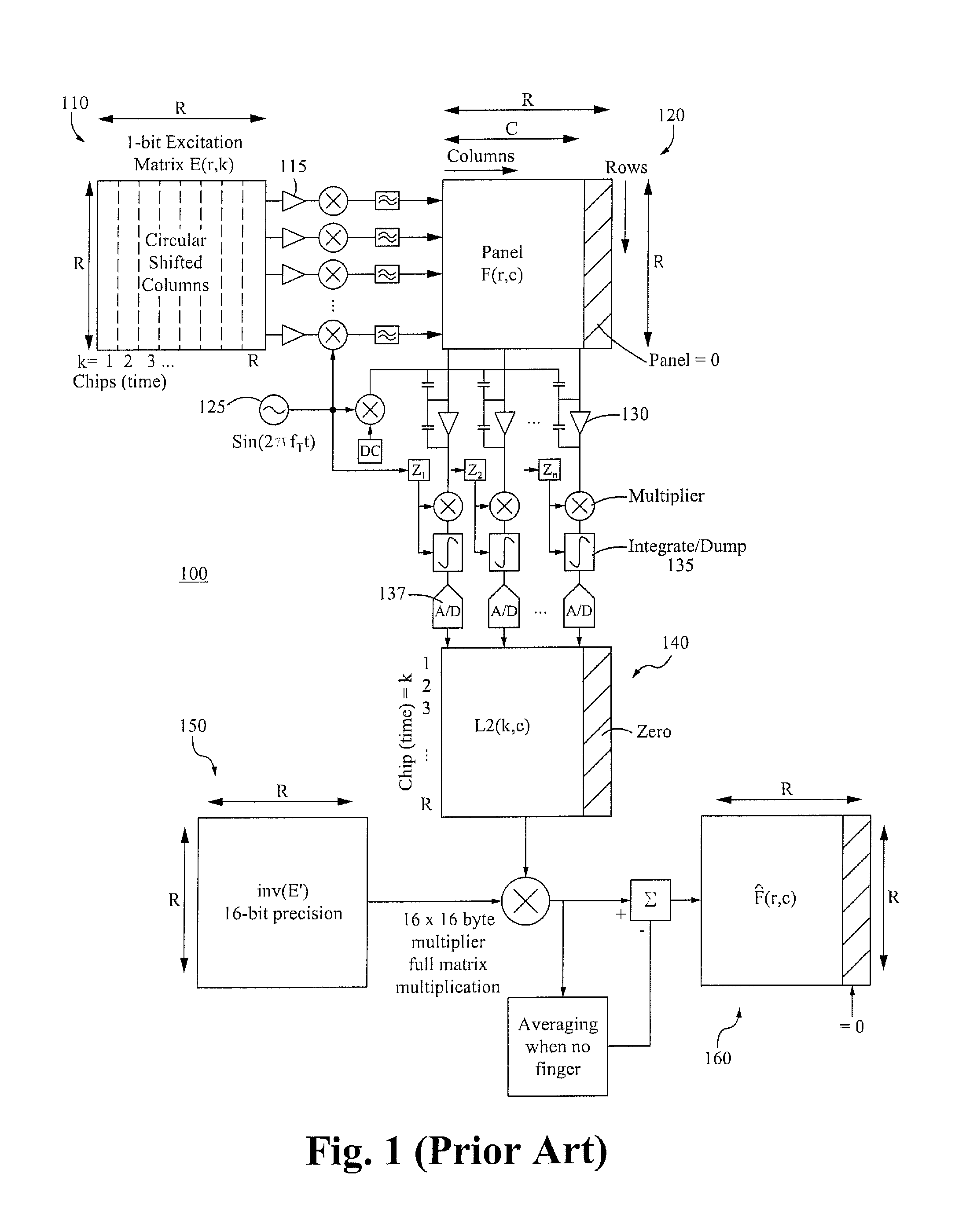
These methods have not been applied to capacitive touch screen systems where the analog signals are stationary and the touch information has a very small impact on the signals.
While digital communication systems can tolerate a large ISI as long as the BER is acceptable, touch screen systems can only tolerate extremely small ISI on the panel analog signal, and therefore they require very special treatment for digital filtering.

Method used


Image

  • Digital filtering and spread spectrum based interference mitigation for mutual and self capacitance panel
  • Digital filtering and spread spectrum based interference mitigation for mutual and self capacitance panel
  • Digital filtering and spread spectrum based interference mitigation for mutual and self capacitance panel

Examples


Embodiment Construction

[0043]The following description is presented to enable one of ordinary skill in the art to make and use the invention and is provided in the context of a patent application and its requirements. Various modifications to the described embodiments will be readily apparent to those skilled in the art and the generic principles herein can be applied to other embodiments. Thus, the present invention is not intended to be limited to the embodiment shown but is to be accorded the widest scope consistent with the principles and features described herein.

[0044]The present invention can be provided as a computer program product that can include a machine-readable medium having stored thereon instructions that can be used to program a computer (or other electronic devices) to perform a process according to the present invention. The machine-readable medium can include, but is not limited to, floppy diskettes, optical disks, CD-ROMs, ROMs, RAMs, magnet or optical cards, or other type of media / m...


PUM


Abstract

A touch screen controller for a capacitive touch screen panel having row conductors intersecting column conductors to form pixels, the touch screen controller comprising: a transmitting unit configured to drive the row conductors with signals formed from an excitation matrix, and a receiving unit configured to sense signals from the column conductors and to determine the capacitance of the pixels using the sensed signals. In some embodiments, the receiving unit is configured to apply zero-ISI filtering to the sensed signals prior to the capacitance of the pixels being determined. In some embodiments, the transmitting unit is configured to spread each bit of the row drive signals with a pseudo-noise code, and the receiving unit is configured to de-spread the sensed signals with the pseudo-noise code. In some embodiments, the transmitting unit is configured to pulse shape the row drive signals.

Description

FIELD OF THE INVENTION[0001]The present invention relates to the field of touch screens. More specifically, the present invention relates to interference mitigation for touch screens.BACKGROUND OF THE INVENTION[0002]Many modern electronic devices incorporate a touch screen to display information and as an input that is activated by touching the display. One technology for implementing the touch aspect of a touch screen is capacitance sensing. An insulator, such as glass, is coated with a transparent conductor, such as indium tin oxide (ITO). Since the human body is an electrical conductor, when a finger actuates the touch screen, such as by touching or even getting very close to its surface, the electrostatic field of the touch screen is distorted, resulting in a measurable change in capacitance.[0003]A mutual capacitance touch screen comprises two layers of material arranged in an X-Y grid such that an actuation of the touch screen can be resolved into a coordinate. A finger is typ...

Claims


Application Information

Patent Timeline
IPC IPC(8): G06F3/045G06F3/041
CPCG06F3/04166G06F3/04182G06F3/0446
Inventor MOHINDRA, RISHI
Owner QUALCOMM INC
Learn More