Semiconductor device

a semiconductor device and semiconductor technology, applied in the field of semiconductor devices, can solve the problems of difficulty in repairing defects in semiconductor devices using alloy processes, complex and finer process of designing and manufacturing semiconductor devices, etc., and achieve the effect of preventing or inhibiting damage to metal interconnections and improving efficiency of alloy processes

Active Publication Date: 2015-03-24
SAMSUNG ELECTRONICS CO LTD
View PDF13 Cites 1 Cited by
  • Summary
  • Abstract
  • Description
  • Claims
  • Application Information

AI Technical Summary

Benefits of technology

[0006]Example embodiments of the inventive concepts provide a semiconductor device capable of sufficiently securing a moving path of hydrogen gas, thereby improving efficiency of an alloy process and preventing or inhibiting damage to a metal interconnection.

Problems solved by technology

However, as a demand for highly functional and compact semiconductor devices increases, processes of designing and manufacturing a semiconductor device become complicated and finer.
Thus, repairing defects in a semiconductor device by using the alloy process may be difficult.

Method used


Image

  • Semiconductor device
  • Semiconductor device
  • Semiconductor device

Examples


Embodiment Construction

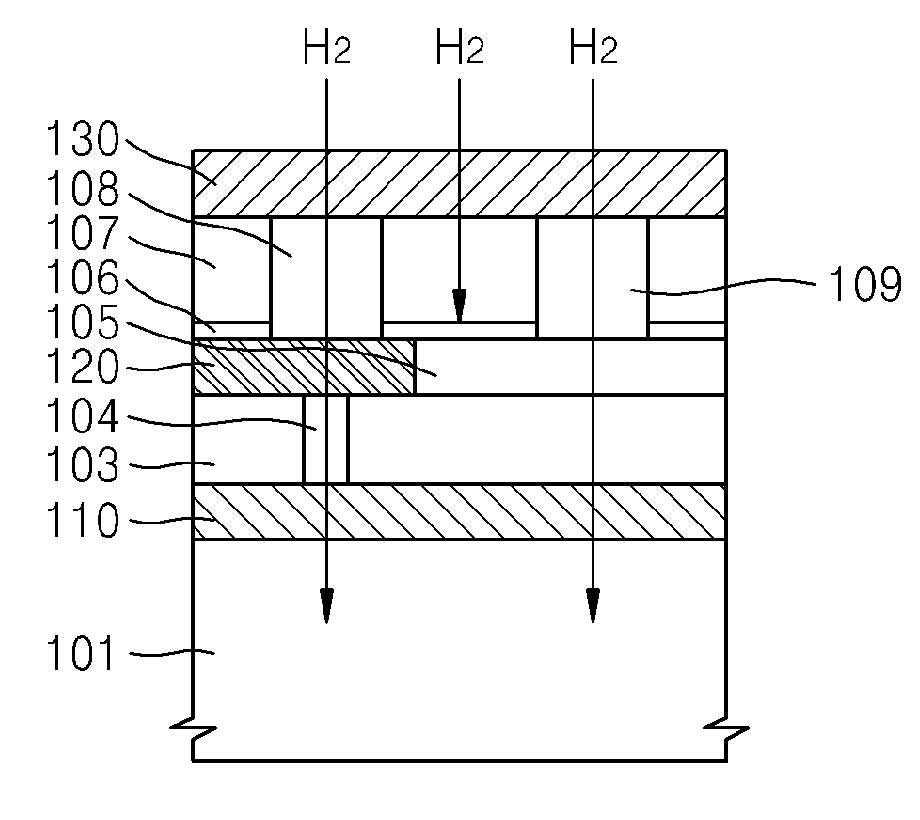
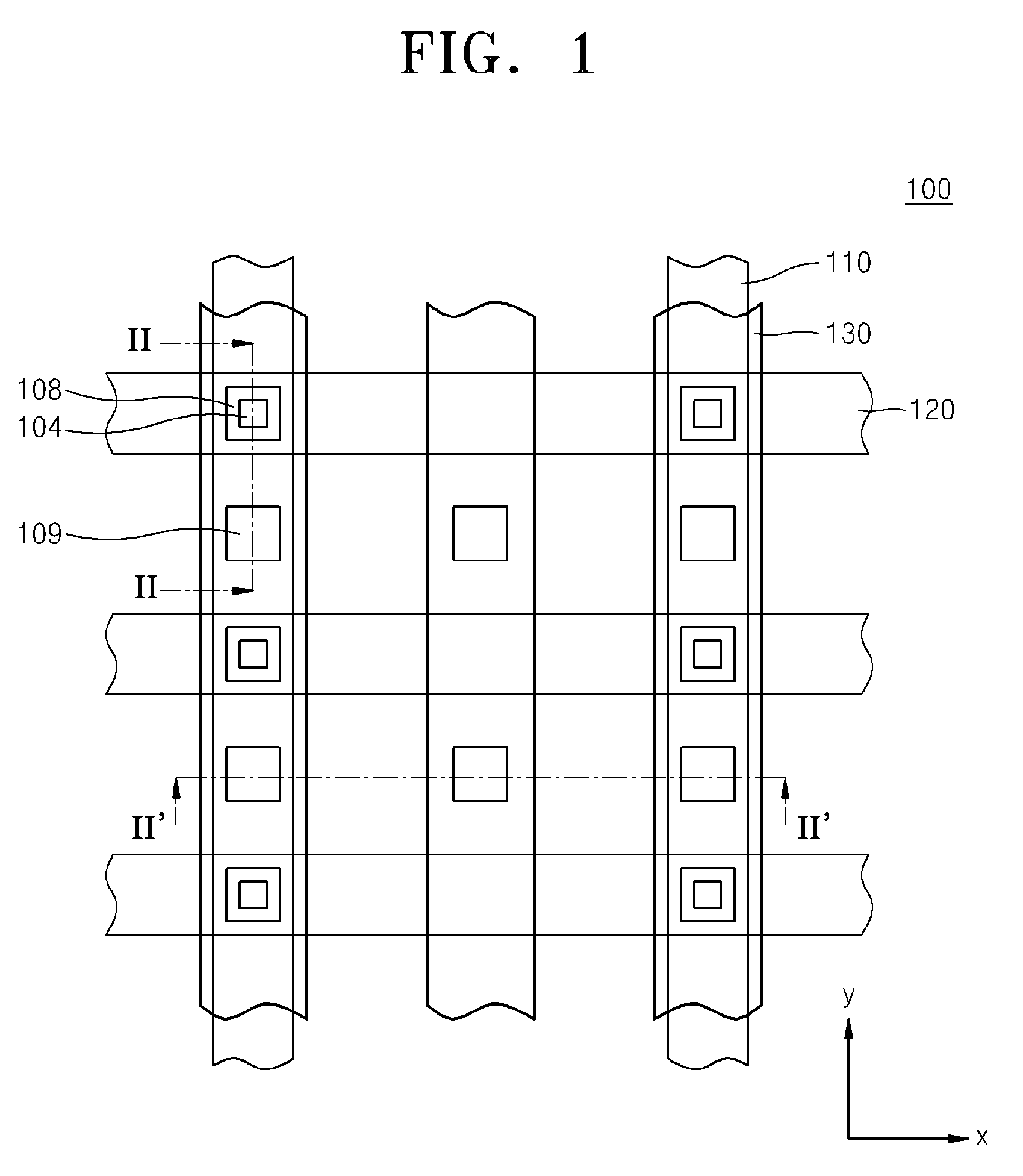
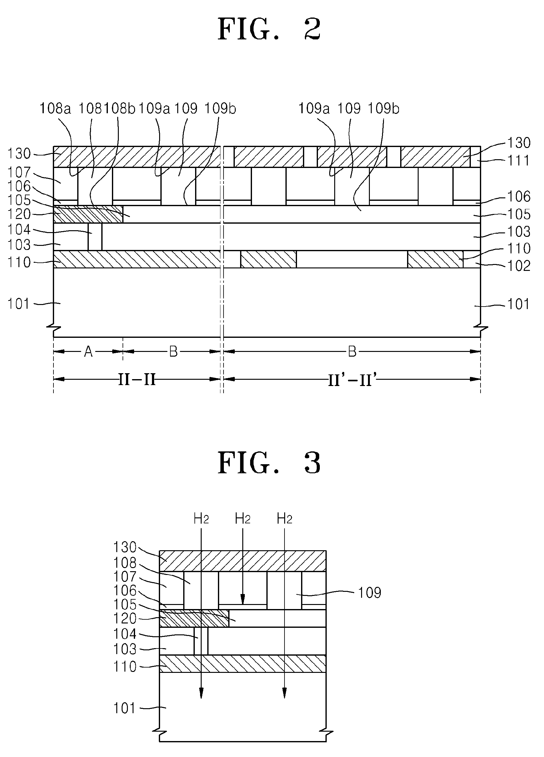
[0036]Hereinafter, the inventive concepts will be described more fully with reference to the accompanying drawings, in which example embodiments of the inventive concepts are shown. The inventive concepts may, however, be embodied in many different forms and should not be construed as limited to the example embodiments set forth herein. Rather, these example embodiments are provided so that this disclosure will be thorough and complete, and will fully convey the scope of the inventive concepts to those of ordinary skilled in the art. The same reference numerals represent the same elements throughout the drawings. In the drawings, lengths and sizes of layers and regions may be exaggerated for clarity.

[0037]It will be understood that, although the terms ‘first’, ‘second’, ‘third’, etc., may be used herein to describe various elements, components, regions, layers and / or sections, these elements, components, regions, layers and / or sections should not be limited by these terms. These ter...


PUM


Abstract

A semiconductor device may include a semiconductor layer including at least one unit device, a first interconnection on the semiconductor layer and electrically connected to the at least one unit device, a diffusion barrier layer on the first interconnection, an intermetallic dielectric layer on the diffusion barrier layer, a plug in a first region of the intermetallic dielectric layer and passing through the diffusion barrier layer so that a bottom surface thereof contacts the first interconnection, and a first dummy plug in a second region of the intermetallic dielectric layer, passing through the diffusion barrier layer, and disposed apart from the first interconnection so that a bottom surface of the first dummy plug does not contact the first interconnection.

Description

CROSS-REFERENCE TO RELATED APPLICATIONS[0001]This application claims the benefit of Korean Patent Application No. 10-2012-0026607, filed on Mar. 15, 2012, in the Korean Intellectual Property Office, the disclosure of which is incorporated herein in its entirety by reference.BACKGROUND[0002]1. Field[0003]Example embodiments of the inventive concepts relate to a semiconductor device, and more particularly, to a semiconductor device including a dummy plug that provides a moving path of hydrogen gas.[0004]2. Description of the Related Art[0005]Recently, research has been actively conducted on various processes of improving electrical characteristics of a semiconductor device. A representative process among these processes is an alloy process of supplying hydrogen and performing a thermal treatment to repair defects in a semiconductor device during a process of forming a unit device or a metal interconnection process. However, as a demand for highly functional and compact semiconductor d...

Claims


Application Information

Patent Timeline
Patent Type & Authority Patents(United States)
IPC IPC(8): H01L23/48H01L23/52H01L29/40H01L23/522
CPCH01L23/52H01L23/522H01L23/5226H01L2924/0002H01L2924/00H01L21/28H01L21/768
Inventor KANG, MIN-SUNGJANG, SE-MYEONG
Owner SAMSUNG ELECTRONICS CO LTD
Why Eureka
Try Eureka